![]()
![]() Instruction Fetch Unit Decoder:
Instruction Fetch Unit Decoder:

![]()
![]()


![]()
![]()
![]() Fig. 1. Dorado block diagram.
Fig. 1. Dorado block diagram.
This document was made by
OCR from a scan of the technical report. It has not been edited or proofread
and is not meant for human consumption, but only for search engines. To see the
scanned original, replace OCR.htm with Abstract.htm or Abstract.html in the URL
that got you here.
The Memory System of a
High-Performance
Personal Computer
DOUGLAS
W. CLARK, BUTLER W. LAMPSON. AND
KENNETH A. PIER
Abstract—The memory system of the Dorado. a compact high-performance
personal computer, has very high I/O bandwidth, a large paged virtual memory, a cache, and heavily pipelined control; this paper discusses all of these in detail.
Relatively low-speed I/O devices transfer single words to or from the cache;
fast devices, such as a color video display,
transfer directly to or from main storage while the processor uses the cache. Virtual addresses are used
in the cache and for all I/O transfers.
The memory is controlled by a seven-stage pipeline, which can deliver a peak
main-storage bandwidth of 533 million bits/s to service fast I/O devices
and cache misses. Interesting problems of synchronization
and scheduling in this pipeline are discussed. The paper concludes with some performance measurements that
show, among other things, that the cache hit rate is over 99 percent.
Index Terms—Cache, high bandwidth, memory system,
pipeline, scheduling, synchronization.
virtual memory.
1. INTRODUCTION
|
T |
HIS paper
describes the memory system of the Dorado.
a
high-performance compact personal computer. This
section explains the design goals for the Dorado. sketches its overall architecture, and describes the
organization of the memory system. Later sections discuss in detail the cache (Section II), the main storage (Section III),
interactions between the two
(Section IV), and synchronization of the various parallel activities in the system (Section V). The paper concludes with a description of the physical
implementation (Section VI) and some performance measurements (Section
VII).
Manuscript
received May 31, 1980; revised March 22, 1981.
D. W. Clark was with the Xerox Palo Alto
Research Center, Palo Alto, CA 94304. He is now with the Systems Architecture
Group, Digital Equipment Corporation,
Tewksbury, MA 01876.
B. W. Lampson and K. A.
Pier are with the Xerox Palo Alto Research Center, Palo Alto, CA 94304.
A. Goals
A high-performance successor to the Alto computer [21], the Dorado is intended to provide the hardware base for the next generation of computer system research at the Xerox Palo Alto Research Center. The Dorado is a powerful but personal computing system supporting a single user within a programming system that extends from the microinstruction level to an integrated programming environment for a high-level language. It is physically small and quiet enough to occupy space near its users in an office or laboratory setting, and inexpensive enough to be acquired in considerable numbers. These constraints on size, noise, and cost have had a major effect on the design.
The Dorado is designed to rapidly execute programs compiled into a stream of byte codes [19]; the microcode that does this is called an emulator. 13) te code compilers and corresponding microcode emulators exist for Mesa, a Pascal-like system implementation language [7].[ 15], Interlisp, a sophisticated Lisp implementation [5],[20], and Smalltalk, an object-oriented language for experimental programming [8]. A pipelined instruction fetch unit (iFu) in the Dorado fetches bytes from such a stream, decodes them as instructions and operands, and provides the necessary control and data information to the emulator microcode in the processor; it is described in another paper [ 1 1 J. Further support for fast execution comes from a very fast microcycle-60 ns-and a microinstruction set powerful enough to allow interpretation of a simple byte code in a single microcycle; these are described in a paper on the Dorado processor [12]. There is also a cache [2].[13] which has a latency of two cycles, and which can deliver a 16-bit word every cycle.
Another major
goal is to support high-bandwidth input/
0018-9340/81/1000-0715$00.75 © 1981
IEEE
![]()
![]() Instruction Fetch Unit Decoder:
Instruction Fetch Unit Decoder:
![]()
![]()
![]()
![]()
![]() Fig. 1. Dorado block diagram.
Fig. 1. Dorado block diagram.
![]()
![]()
![]()
![]()
![]()
![]()
![]()
![]()
![]() output.
In particular, color monitors, raster scanned printers, and high-speed
communications are all part of the computer research activities within the Palo
Alto Research Center; these devices typically
have bandwidths of 20-400 million bits/s. Fast devices must not excessively degrade program execution, even
though the two functions compete for many of the same resources. Relatively slow devices, such as a keyboard or an Ethernet interface [14], must also be supported
cheaply, without tying up the
high-bandwidth 1/0 system. These considerations
clearly suggest that 1/0 activity and program execution should proceed
in parallel as much as possible. The memory
system therefore allows parallel execution of cache accesses and main storage
references. Its pipeline is fully
segmented: it allows a cache reference to start in every microinstruction cycle (60 ns), and a main storage reference
to start in every main storage cycle
(480 ns).
output.
In particular, color monitors, raster scanned printers, and high-speed
communications are all part of the computer research activities within the Palo
Alto Research Center; these devices typically
have bandwidths of 20-400 million bits/s. Fast devices must not excessively degrade program execution, even
though the two functions compete for many of the same resources. Relatively slow devices, such as a keyboard or an Ethernet interface [14], must also be supported
cheaply, without tying up the
high-bandwidth 1/0 system. These considerations
clearly suggest that 1/0 activity and program execution should proceed
in parallel as much as possible. The memory
system therefore allows parallel execution of cache accesses and main storage
references. Its pipeline is fully
segmented: it allows a cache reference to start in every microinstruction cycle (60 ns), and a main storage reference
to start in every main storage cycle
(480 ns).
The implementation of the Dorado memory reflects
a balance among competing demands:
· for simplicity, so
that it can be made to work initially, and maintained
when components fail;
· for
speed, so that the performance will be well-matched to the rest of the machine;
·
for compactness, since cost and packaging considerations limit the number of components and edgepins that
can be used.
None of these demands is absolute, but all have
thresholds that
are costly to cross. In the Dorado we set a somewhat arbitrary speed requirement for the whole machine, and generally tried to save space by adding complexity,
pushing ever closer to the simplicity threshold. Although many of the complications in the memory system are unavoidable
consequences of the speed requirements, some of them could have been eliminated by adding hardware.
B. Gross
Structure of the Dorado
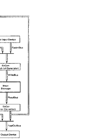
Fig.
1 is a simplified block diagram of the Dorado. Aside from 1/0, the
machine consists of the processor, the IFU. and the memory system. The memory system in turn contains a cache, a hardware virtual-to-real address map, and
main storage. Both the processor and
the IFU can
make memory references and transfer data to and from the memory
through the
cache. Slow, or low-bandwidth I/O devices communicate with the processor, which in turn transfers their data to and from the cache. Fast, or high-bandwidth devices
communicate directly with storage,
bypassing the cache most of the time.
For the most part, data is handled 16 bits at a time. The
relatively narrow buses, registers, data paths, and memories which
result from this choice help to keep the machine compact.
This is especially important for the memory, which has a large number of
buses. Packaging. however, is not the only consideration.
Speed dictates a heavily pipelined structure in any case, and this parallelism in the time domain tends to compensate for the lack of parallelism in the space
domain. Keeping the machine physically small also improves the speed, since physical distance (i.e., wire length)
accounts for a considerable fraction
of the basic cycle time. Finally, performance is often limited by the cache hit rate, which cannot be improved, and
may be reduced, by wider data paths (if the number of bits in the cache is fixed).
Rather than putting processing capability in each
I/O controller and using a shared bus or a switch to access
the memory,
the Dorado shares the processor among all the I/O devices and the emulator. This idea, originally tried in the TX-2 computer [6] and also used in the Alto [21],
works for two main reasons. First, unless a system has both multiple memory buses (i.e., multiported memories) and
multiple memory modules that can cycle independently, the main factor governing processor throughput is memory
contention. Put simply, when I/O devices make memory references, the emulator
ends up waiting for the memory. In this situation the processor might as well be working for the I/O device. Second, complex device interfaces can be implemented with
relatively little dedicated hardware,
since the full power of the processor is
available to each device.
This processor sharing is accomplished with 16 hardware-scheduled
microcode processes, called tasks. Tasks have fixed priority. Most tasks serve a single I/O device, which raises a request
line when it wants service from its task. Hardware schedules the processor so as to serve the highest
priority request; control can switch from one task to another on every
microinstruction, without any cost in time. When no device is requesting service. the lowest priority task runs
and does high-level language
emulation. To eliminate the time cost of multiplexing the processor among the tasks in this way, a number of the machine's working registers are task-specific, i.e., there is a copy for each task.
The implementation typically involves a
single physical register, and a 16-element memory which is addressed by the current task number and
whose output is held in the register.
Many design decisions were
based on the need for speed.
Raw circuit speed certainly comes first. Thus, the Dorado
is implemented using the fastest commercially available technology
that has a reasonable level of integration and is not too hard
to package. When our design was started in 1976, the obvious
choice was the ECL (emitter-coupled logic) 10K family of
integrated circuits. These circuits make it possible for the Dorado to
execute a microinstruction in 60 ns. Second, there
are several pipelines, and they are generally able to start a new operation every cycle. The memory, for
instance, has two pipelines, the processor two, the instruction fetch unit
another. Third, there are many
independent buses: eight in the memory, half a dozen in the processor. three in the IFU. These buses increase
bandwidth and simplify scheduling, as will be seen in
later sections of the paper.
C. Memory
Architecture
The paged virtual memory of the Dorado is designed to accommodate
evolving memory chip technology in both the address
map and main storage. Possible configurations range from the current 22-bit virtual address with l 6K
256-word pages and up to one million
words of storage (using 16K chips in
both map and storage) to the ultimate 28-bit virtual address with 256K 1024-word pages and 16 million words of
storage (using 256K chips). All
address buses are wired for their maximum size, so that configuration
changes can be made with chip replacement
only.
The addressable unit of memory is the 16-bit word. Memory references specify a 16 or 28 bit displacement and, by means of a
task-specific register, one of 32 base
registers of 28 bits; the virtual address
is the sum of the displacement and the base.
Virtual address translation, or mapping, is implemented by
table look-up in a dedicated memory. Main storage is the permanent
home of data stored by the memory system. Storage is
slow (i.e., it has long latency, which means that it takes a long time to respond to a
request) because of its implementation in cheap
but relatively slow dynamic MOS RAM's (random access memories). To make up for being slow, storage is big and
has high bandwidth. which is more important than latency for sequential
references. In addition, there is a cache which services
nonsequential references with high speed (low latency), but is inferior to main storage in its other
parameters. The relative values of
these parameters are shown in Table 1.
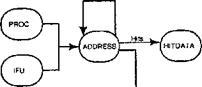
With one exception (the IFU), all memory
references are initiated by microcode in the processor, which thus acts as a multiplexor controlling access to the memory (see
Section I-B and [12]) and serves as
the sole source of addresses. Once started, however, a reference
proceeds independently of the processor.
Each one carries with it the number of its originating task, which serves to identify the source or sink
of any data transfer associated with the reference. The actual transfer
may take place much later, and each source or
sink must be continually ready to deliver or accept data on demand. It is possible
for a task to have several references outstanding, but order is preserved within each type of reference, so that
the task number plus some careful
hardware bookkeeping is sufficient to match up data with references.
Table II lists the types of memory references
executable by
TABLE I
PARAMETERS OF THE CACHE RELATIVE TO STORAGE
|
|
|
|
|
|
|
|
|
|
|
Cache 1 1 |
|
Storage 15 2 250 |
|
|
Latency
Bandwidth Capacity |
|
|
||
|
|
|
|
|
|
|
TABLE II
MEMORY-REFERENCE INSTRUCTIONS
AVAILABLE TO MICROCODE
![]() Reference Task Effect
Reference Task Effect
![]() fetchta) any task latches
one word of data from sMual address
fetchta) any task latches
one word of data from sMual address
a in the cache and
delivers it to FetchReg register
storc(d.
a) any task stores
data ward d at virtual
address a M-the
cache
I/Oreac(a) I/O task only reads
block at virtual address a in storage
and delivers it to a
fast output device
1/0..crice(a) I/O task only takes a
block from a fast input device
and writes it at
rirtual address a in
storage
preletch(a) any task loads
the cache from sturage with the block
at virtual address a
flush(a) emulator only removes
from the cache (re-writing to storage
if necessary) the
black at virtual address a
mapRead(u) emulator only reads
the map entry addressed by
virtual address a
mapWrite(d,
a) emulator only antes d:nto the map entry addressed by
virtaal address a
dvrnmyRef(a) any task makes
a pseudo-reference guaranteed not to
reference storage
or alter the cache (useful fc, diagnostics)
![]() microcode. Fig. 2, a
picture of the memory system's main data paths,
should clarify the sources and destinations of data transferred by these references (parts of Fig. 2
will be explained in more detail later). All references, including fast
I/O references, specify virtual, not real
addresses. Although a microinstruction actually specifies a displacement and a
base register which together form the
virtual address, for convenience we
will suppress this fact and write, for example, fetch(a) to mean a fetch from virtual address a.
microcode. Fig. 2, a
picture of the memory system's main data paths,
should clarify the sources and destinations of data transferred by these references (parts of Fig. 2
will be explained in more detail later). All references, including fast
I/O references, specify virtual, not real
addresses. Although a microinstruction actually specifies a displacement and a
base register which together form the
virtual address, for convenience we
will suppress this fact and write, for example, fetch(a) to mean a fetch from virtual address a.
A fetch
from the cache delivers data to a register called FetchReg, from which it can be
retrieved at any later time; since FetchReg is
task-specific, separate tasks can make their cache references independently. An
1/Dread reference
delivers a 16-word block
of data from storage to the FastOutBus (by way of the error
corrector, as shown in Fig. 2), tagged with the identity of the requesting task; the associated output device is expected to monitor this bus and grab the data
when it appears. Similarly, the processor can store one word of data into the cache, or do an 110write
reference,
which demands a block of data from an input
device and sends it to storage (by way of the check-bit generator).
There is also a prefetch reference, which brings a block into the cache
without delivering data to FetchReg and
without causing the processor to wait in the event of a cache miss. Prefetch
can therefore be used to advantage when the microcode can anticipate the need
for a particular block. Fetch, store,
and prefetch are called cache
references. There are special references to flush data from the cache and to allow map entries to be read and
written; these will be discussed later.
The IFU is the only device
that can make a reference independently of
the processor. It uses a single base register, and is treated almost exactly like a processor cache
fetch, except that the IFU has its own set of registers for receiving
memory data (see [11] for details). In
general, we ignore IFU references
Cache Data Paths Storage
Data Paths
|
I I |
|
from Processor

![]()
![]()
![]()
![]()
![]()
![]()
![]()
![]()
![]()
![]() Fig. 2. Memory
system data paths.
Fig. 2. Memory
system data paths.
from now on, since they add little complexity to the memory system.
A cache reference usually hits: i.e., it finds the
referenced word in the cache. If it misses (does not find the word), a
main storage operation must
be done to bring the block containing the requested word into the
cache. In addition, fast I/O references always do storage operations. There are
two kinds of storage operations, read and write, and we will generally use these
words only for storage operations in order to distinguish them from the
references made by the processor. The former transfers
a block out of storage to the cache or I/O system; the latter transfers a block into storage from the
cache or I/O system. All storage
operations are block-aligned.
D. Implementation for High
Performance
Two major forms of concurrency make it possible to implement
the memory system's functions with high performance.
Physical: The
cache (8K-32K bytes) and the main storage (0.5M-32M bytes) are almost
independent. Normally, programs execute from the cache, and fast I/O
devices transfer to and from the storage. Of course, there must
be some coupling when a program refers to data that are not in the
cache, or when I/O touches data that are: this is the subject
of Section IV.
Temporal: Both cache and storage are implemented by fully
segmented
pipelines. Each can accept a new operation once per cycle of the
memory involved: every machine cycle (60 ns) for the cache, and every eight machine
cycles (480 ns) for the storage.
To support this concurrency, the memory has
independent buses for cache and main storage addressing (2), data
into and out of the cache (2) and main storage (2), and fast input
and output (2). The data buses, but not the address buses, are
visible in Fig. 2. It is possible for all eight buses to
be active in a single cycle, and under peak load
sustained utilization of five or six of them can be achieved. In general, there
are enough buses
that an operation never has to wait for a bus; thus the problems of concurrently scheduling complex operations that share many resources are simplified by reducing the
number of shared resources to the
unavoidable minimum of the storage devices
themselves.
All buses are 16 bits wide; blocks of data are
transferred to and from storage at the rate of 16 bits every half cycle (30
ns). This means that 256 bits can be transferred in 8 cycles or 480 ns,
which is approximately the cycle time of the RAM chips that implement main
storage. Thus, a block size of 256 bits provides a good match
between bus and chip bandwidths; it is also a reasonable unit
to store in the cache. The narrow buses increase the latency of a
storage transfer somewhat, but they have little effect on the
bandwidth. A few hundred nanoseconds of latency is of little
importance either for sequential I/O transfers or for delivery
of data to a properly functioning cache.
Various measures are taken to maximize the
performance of the cache. Data stored there is not written back to
main storage until the cache space is needed for some other
purpose (the
write-back rather than the more common write-through discipline
[1], [16]); this makes it possible to use memory locations much like registers
in an interpreted instruction set, without incurring the penalty of main storage
accesses. Virtual rather than real addresses
are stored in the cache, so that the speed of memory mapping does not affect
the speed of the cache references. (Translation buffers [17], [23] are another way to accomplish this.) This would create problems
if there were multiple address
spaces. Although these problems can be
solved, in a single-user environment with a single address space they do
not even need to be considered.
Another important technique for speeding up data
manipulation
in general, and cache references in particular, is called bypassing. Bypassing is one of
the speed-up techniques used in the common data bus of the IBM 360/91 [22].
Sequences of instructions having the form
1)
register computation l
2)
computation2 involving the register
are very common. Usually the execution of the first
instruction takes more than one cycle and is pipelined. As a result,
however,
the register is not loaded at the end of the first cycle, and therefore is not ready at the beginning of the
second instruction. The idea of
bypassing is to avoid waiting for the register to be loaded, by routing the results of the first computation directly to
the inputs of the second one. The effective latency of the cache can thus be reduced from two cycles to
one in many cases (see Section I
I-C).
|
|
Cache pipeline |
|
1 |
|
|
|
||
|
Dirty Victim |
|
|
|
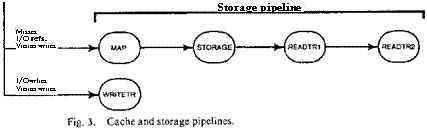

The memory system is organized into two kinds of building blocks: pipeline stages, which provide the control (their names are
in SMALL CAPITALS), and resources, which
provide the data paths and memories. Fig. 3
shows the various stages and their
arrangement into two pipelines. One, consisting of the ADDRESS and HITDATA stages, handles cache references and is the subject of the next section; the other,
containing MAP. WRITETR, STORAGE, READTRI, and READTR2, takes care of storage references and is dealt with in
Sections III and IV. References
start out either in PROC, the
processor, or in the IFU.
As
Fig. 3 suggests, there are no queues between pipeline stages. Passage of a
reference from one stage to the next requires the second stage to be empty or about to become empty. Each stage handles one reference at a time.
II. THE CACHE
The
cache pipeline's two resources, CacheA
and CacheD, correspond roughly to its two stages, although each is also used by other stages in the storage pipeline. CacheA
stores addresses and associated flags, and contains
the comparators which decide whether a given address is currently in the cache.
CacheD stores cache data. Fig. 4 shows the
data paths and memories of these
resources. The numbers on the left side of the figure indicate the time at which a reference reaches each point in the pipeline, relative to the start of
the microinstruction making the reference.
Every
reference is first handled by the ADDRESS stage, whether or not it involves a cache data transfer.
The stage calculates the virtual address and checks to see whether the
associated data is in the
cache. If it is (a hit), and the reference is a fetch or store. ADDRESS starts HITDATA, which is responsible for the one-word data transfer. On a cache reference that misses, and on any I/O reference, ADDRESS starts MAP, as
described in Section III.
HITDATA obtains the cache address of the word being referenced from ADDRESS, sends this address to CacheD, which holds the cache data, and either fetches a word
and delivers it to the FetchReg
register of the task that made the reference, or stores the data delivered by the processor via the
StoreReg register.
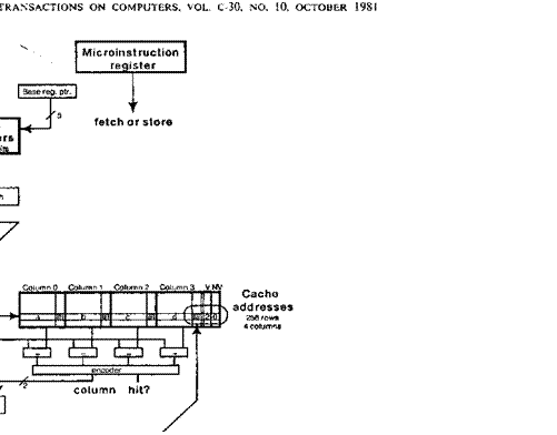
A. Cache Addressing
Each
reference begins by adding the contents of a base register to a displacement provided by the processor (or IFU). A task-specific register holds a 5-bit pointer
to a task's current base register. These pointers, as well as the base
registers themselves, can be changed by
microcode.
Normally
the displacement is 16 bits, but by using both its buses the processor can supply a full 28-bit
displacement. The resulting
sum is the virtual address for the reference. It is divided into a 16-bit key, an 8-bit row number, and a 4-bit word number;
Fig. 4 illustrates this. This division reflects the physical structure of the cache, which consists of 256 rows, each capable of holding four independent 16-word
blocks of data, one in each of four columns. A given address determines a row (based on its 8 row bits), and it must appear in some column of that row if it is in the cache at all.
For each row, CacheA stores the
keys of the four blocks currently in that row, together with four flag bits for each block. The Dorado
cache is therefore set-associative [3]; rows correspond to sets and columns to the elements of a set.
Given this
organization, it is simple to determine whether an address is in the cache. Its row bits are used to select a row, and the four keys stored there are compared with
the given address. If one of them matches, there is a hit and the address has been located in the cache. The number of the
column that matched, together with
the row bits, identifies the block completely,
and the four bits of the address select one of the 16 words within that block. If no key matches,
there is a miss: the address is not present in the cache. During normal operation. it is not possible for more than one column
to match. The entire matching process
can be seen in Fig. 4, between 60 and 90
ns after the start of the reference_ The cache address latched at 90 ns contains the row, word, and column; these
14 bits address a single \A ord in
CacheD. Of course, only the top 16 key
bits of the address need be matched, since the row bits are used to select the row, and all the words of a
block are present or absent together.
Four
flag bits are stored with each cache entry to keep track of its status. We defer discussion of these
flags until Section IV.


![]()
![]()
![]()
![]()
![]()
![]()
![]()
![]()
![]()
![]()
![]()
![]()
![]()
![]()
![]()
![]()
![]()
![]()
![]()
![]()
![]()
![]()
![]()
![]()
![]()


![]()
![]()
![]()
![]()
![]()
![]()
![]()
![]()
![]()
![]() CacheD
CacheD
120
150
Fig. 4. Data paths in the
cache. Numbers beside diagonal marks are widths in bits.
![]()
 FetchRegRAM entry for the new task is read out
and loaded into FetchReg. Matters are further complicated by the bypassing
scheme described in the next subsection.
FetchRegRAM entry for the new task is read out
and loaded into FetchReg. Matters are further complicated by the bypassing
scheme described in the next subsection.
StoreReg is not task-specific. The reason for
this choice and the problem it causes are explained in Section V-A.
C.
Cache Pipelining
From the beginning of a cache reference, it takes
two and a
half cycles before the data is ready in FetchReg, even if it hits and there are
no delays. However, because of the latches in the pipeline (some of which are omitted from Fig. 4) a new reference
can be started every cycle; thus the ADDRESS stage, which appears in Fig. 4 to take 90 ns or one and one-half
cycles to operate, can be thought of
as working in one cycle. If there are no misses the pipeline will never
clog up, but will continue to deliver a word
every 60 ns. This works because nothing in later stages of the pipeline affects anything that happens in an earlier stage.
The exception to this principle is delivery of
data to the processor itself. When the processor uses data that has been fetched,
it depends on the later stages of the pipeline. In general,
this dependency is unavoidable, but in the case of the cache
the bypassing technique described in Section I-D is used to
reduce the latency. A cache reference logically delivers its
data to the FetchReg register at the end of the cycle following the reference cycle (actually halfway through the second cycle. at 150 in Fig. 4). Often the data is then sent to a register in the processor, with a microcode sequence such as
1) fetch(address)
2) register 4—• FetchReg
3) ALU computation involving register.
The register is not actually loaded until cycle 3); hence its data, which is ready in the middle of cycle 3), arrives in time, and instruction 2) does not have to wait. The data is supplied to the computation in cycle 3) by bypassing the register. The effective latency of the cache is thus only one cycle in this situation.
Unfortunately, this sleight-of-hand does not always work. The sequence
1) fetch(address)
2) ALU computation involving FetchReg
actually needs the data during cycle 2). The ALU computation cannot be bypassed, as can the mere loading of a register. Microinstruction 2) will therefore have to wait for one cycle (see Section V-A).
Data retrieved in cycle 1) would be the old value
of FetchReg. This allows a sequence of
fetches
1) fetch (address 1 )
2) register 1 FetchReg, fetch(address2)
3) register2 FetchReg, fetch(address3)
4)
register3 FetchReg,
fetch(address4)
· •
to proceed at full speed.
III. STRUCTURE AND OPERATION OF THE
STORAGE
PIPELINE
Cache misses
and fast I/O references use the storage portion of the pipeline, shown in Fig.
3. In this section we first describe the
operation of the individual pipeline stages, then explain how fast I/O
references use them, and finally discuss how memory faults are handled. Using I/O references to expose the workings of the
pipeline allows us to postpone until Section IV a close examination of the more complicated
references involving both cache and
storage.
A. Pipeline Stages
Each of the pipeline stages is implemented by a simple finite-state automaton that can change state on every microinstruction cycle. Resources used by a stage are controlled by signals that its automaton produces. Each stage owns some resources, and some stages share resources with others. Control is passed from one stage to the next when the first produces a start signal for the second; this signal forces the second automaton into its initial state. Necessary information about the reference type is also passed along when one stage starts another.
The ADDRESS Stage: As we saw in Section II, the ADDRESS stage computes a reference's virtual address and looks it up in CacheA. If it hits, and is not I/Oread or I/Owrite, control is passed to HITDATA. Otherwise, control is passed to MAP.starting a storage cycle. In the simplest case a reference spends just one microinstruction cycle in ADDRESS, but it can be delayed for various reasons discussed in Section V.
The MAP Stage: The MAP stage translates a virtual address into a real address by looking it up in a dedicated hardware table called the MapRAM, and then starts the STORAGE stage. Fig. 5 illustrates the straightforward conversion of a virtual page number into a real page number. The low-order bits are not mapped; they point to a single word on the page.
Three flag bits are stored in MapRAM for each virtual page:
· ref, set
automatically by any reference to the page;
· dirty, set automatically by any write into the page;
· writeProtect. set by memory-management software (using the mapWrite reference).
A virtual page not in use is marked as vacant by setting both writeProtect and dirty, an otherwise nonsensical combination. A reference is aborted by the hardware if it touches a vacant page, attempts to write a write-protected page, or causes a parity error in the MapRAM. All three kinds of map fault are passed down the pipeline to READTR2 for reporting.
MAP takes eight cycles to complete. MapRAM outputs are available for the STORAGE stage in the fifth cycle; the last three cycles are used to rewrite the flags. MapRAM entries (including flags) are written by the mapWrite reference. They are read by the mapRead reference in a slightly devious way explained in Section III-C.
The STORAGE Stage: The Dorado's main storage, a resource called StorageRAM, is controlled by the STORAGE stage. STORAGE is started by MAP, which supplies the real storage address and the operation type-read or write. StorageRAM is organized into 16-word blocks, and the transfer of a block is called a transport. All references to storage involve an entire block. Transports into or out of the StorageRAM take place on word-sized buses called ReadBus and WriteBus. Block-sized shift registers called ReadReg and WriteReg lie between these buses and StorageRAM. When storage is read, an entire block (256 bits plus 32 error-correction bits) is loaded into ReadReg all at once, and then transported to the cache or to a fast output device by shifting words sequentially out of ReadReg at the rate of one word every half-cycle (30 ns). On a write, the block is shifted a word at a time into WriteReg, and when the transport is finished, the 288 storage chips involved in that block are written all at once. Fig. 6 shows one bit-slice of WriteReg, StorageRAM, and ReadReg (neglecting the error-correction bits); 16 such bit-slices comprise one storage module, of which there can be up to four. Fig. 2 puts Fig. 6 into context.
WriteR. and ReadReg are not owned by STORAGE, and it
is therefore possible to overlap consecutive storage operations. Furthermore, because the eight-cycle (480
ns) duration of a transport approximates the 375 ns cycle time of the
16K MOS RAM chips. it is possible to keep StorageRAM busy essentially all the time. The resulting bandwidth
is one block every eight cycles, or 533 million bitsfs. ReadReg is shared
between STORAGE, which loads it,
and READTRI /2, which shift it. Similarly, WriteReg is shared
between WRITETR,
![]()

![]()
![]()
![]()
![]()
![]()
![]()
![]()
![]()
![]()
![]() VIRTUAL PAGE
VIRTUAL PAGE
18
(14)
WORD Cal PAGE
REAL PAGE NUMBER FLAGS
![]() MapRAM 2565 (165)
MapRAM 2565 (165)
![]()
![]()
![]()
![]() + ++ 14(12) re!
WP dirty
+ ++ 14(12) re!
WP dirty
![]() REAL ADDRESS 24 BITS
(20)
REAL ADDRESS 24 BITS
(20)
![]() 2 18(14)
2 18(14)
MODULE STORAGE
CHIP
ADDRESS
![]() Fig. 5. Virtual address to real
address mapping. The notation n(m) means that with current RAM chips the
value is m; with future chips the value will be n, for which the boards are wired.
Fig. 5. Virtual address to real
address mapping. The notation n(m) means that with current RAM chips the
value is m; with future chips the value will be n, for which the boards are wired.

![]()
![]() WriteReg
WriteReg
![]() 111
111
B40
of word 15 14 13
ITT
16 bit
serial . parallel-out OM! register
![]()
![]()
![]()
![]() StorageRAM
StorageRAM
MOS RAMS
![]() 16K, 64K, Cr 256K by l bit
16K, 64K, Cr 256K by l bit
|
ReadReg |
16 bit parallel-in, serial-out shift register |
|
Read8us |
|
|
8110 |
||
|
|
|
|
|
Fig 6. One
bit-slice of StorageRAM and its data registers.
which
loads it, and STORAGE, which
writes the data into the RAM chips and releases it when their hold time has
expired.
Each
storage module has capacity 256K, 1 M, or 4M 16-bit words, depending on whether 16K,
64K, or (hypothetical) 256K RAM
chips are used. The two high-order bits of the real address select the module
(see Fig. 5); modules do not run in parallel. A standard Hamming error-correcting code is used, capable of correcting single errors and
detecting double errors in four-word groups. Eight check bits, therefore, are
stored with each quad word; in what follows we will often ignore these bits.
The WRITETR Stage:
The WRITETR stage transports a block into WriteReg, either from CacheD or from an input device. It owns ECGen, the Hamming check bit generator, and WriteBus,
and shares WriteReg with STORAGE.
It is started by
ADDRESS
on every write, and
synchronizes with STORAGE, as explained in Section V-C, It runs for 11 cycles on an I/ Owrite, and for twelve cycles on a cache write,
As Fig, 3 shows, it starts no subsequent
stages itself.
The READTRI
and READTR2 Stages:
Once ReadReg is loaded by STORAGE,
the block is ready for transport to CacheD or to a fast output device. Because it must
pass through the error corrector EcCor, the
first word appears on ReadBus
three cycles before the first corrected word appears at the input to CacheD or on the FastOut bus
(see Fig. 2). Thus, there are
at least 11 cycles of activity related to readtransport,
and controlling the entire transport with a single stage would limit the rate at which read transports could be done to one every 11 cycles. No such limit is
imposed by the data paths, since the
error corrector is itself pipelined and does not require any wait between quadwords or blocks. To match the storage,
bus, and error corrector bandwidths, read transport must be controlled by two eight-cycle stages in series; they
are
called READTRI and READTR2.
In
fact, these stages run on every storage operation, not just on reads. There are several reasons for this.
First, READTR2
reports faults (page faults, map parity errors, error corrections) and wakes up the fault-handling microtask
if necessary (see Section III-C); this must be done for a write as well as for a read. Second, hardware is saved by making all
operations flow through the
pipeline in the same way. Third, storage bandwidth is in any case limited by the transport time and the StorageRAM's cycle time. Finishing a write
sooner would not reduce
the latency of a read, and nothing ever waits for a write to complete.
On a
read, STORAGE
starts READTRI just as it parallel-loads ReadReg with a block to be transported. READTR1 starts shifting words out of ReadReg and through the error corrector. On a write, READTR
I is started at the same point, but no transport is done. READTRI starts READTR2, which shares with it responsibility for controlling the transport and the error corrector. READTR2 reports faults (Section III-C) and corn‑

![]()
![]()

![]()
![]() pletes cache read operations either by delivering the requested
word into FetchReg (for a fetch), or by storing the contents of StoreReg into the newly loaded block in the
cache (for a store).
pletes cache read operations either by delivering the requested
word into FetchReg (for a fetch), or by storing the contents of StoreReg into the newly loaded block in the
cache (for a store).
B. Fast I/O References
We now
look in detail at simple cases of the fast 1/0 references I/Oread and I/Owrite. These references
proceed almost independently of
the cache, and are therefore easier to understand than fetch and store
references, which may involve both the cache and
storage.
The reference I/Oread(x)
delivers a block of data from virtual location x to a fast output device. Fig. 7 shows its progress through the memory system; time divisions on the horizontal axis correspond to microinstruction
cycles (60 ns). At the top is the
flow of the reference through the pipeline: in the middle is a time line annotated with the major events of the reference; at the bottom is a block diagram of the
resources used. The same time scale is used in all three parts, so that a
vertical section shows the stages, the major events, and the resources in use
at a particular time. Most of the stages pass through eight states,
labeled 0-7 in the figure_
The
I/Oread spends one cycle in the processor and then one in ADDRESS. during which x is computed (base register plus
displacement) and looked up in CacheA. We assume for the moment that x misses; what
happens if it hits is the subject of Section
IV-D. ADDRESS starts MAP, passing it x. MAP translates x into the real
address r and starts STORAGE, passing it r;
MAP
then spends three more
cycles rewriting the flags
as appropriate and completing the MapRAM cycle. STORAGE does a StorageRAM
access and loads the 16-word block of data
(together with its check bits) into ReadReg.
It then starts READTRI and
completes the StorageRAM cycle. READTRI and READTR2 transport
the data, control the error
corrector, and deliver the data to FastOutBus. Fault reporting, if necessary, is done by READTR2 as soon as the condition of the last quadword in
the block is known.
It is
clear from Fig. 7 that an I/Oread can be started every eight machine cycles,
since this is the longest period of activity of any stage. This would result in
533 million bits/s of bandwidth,
the maximum supportable by the memory system. The inner loop of a fast I/O task
can be written in two microinstructions,
so if a new I/Oread is launched every eight cycles, one-fourth of the processor capacity will be
used. Because ADDRESS is used for only one cycle per I/Oread, other
tasks–notably the emulator–may continue to hit in the cache when the I/O task is not running.
I/Owrite(x) writes into virtual location x a block of data delivered by a fast input device, together with
appropriate Hamming code check bits. The data always goes to storage, never to the cache, but if address x happens to hit in the cache, the entry is invalidated by setting a flag (Section IV). Fig. 8 shows
that an I/Owrite proceeds through the pipeline very much like an I/Oread. The difference, of course,
is that the WRITETR stage runs, and the READTR1 and READTR2
CileCk VA MapRAM Map SlorageRAM data in error-corrected block c n
in Caches read data out read ReadReg FastOD/Bus
![]()
![]()
![]()
![]()
![]()
![]()
![]()
![]()
![]() Read
Read
![]() Reg I
ReadRes ______________ see,cosses
Reg I
ReadRes ______________ see,cosses
![]() Fig. 7. An t/Oread
reference.
Fig. 7. An t/Oread
reference.

![]() 0 t2 314 IS Is I7 18 Is 1,01
0 t2 314 IS Is I7 18 Is 1,01
announc=
f 12 1 3 I. 1 s I 7 i
101,1213101516171
101,1213141516171
block co block
in
INrsteBes VoiteReg clan!:
rep rang
![]() bine
bine
check VA
Fba'stInElousn write Signal
in
Cache' to
StorageRAM
|
bees Input demsce |
|
|
|
|
Fast! Sus |
E_Gen |
C We. WriteRtro Reg |
|
|
|
|
||
|
|
|
|
|
![]()
![]()
![]()
![]()
![]()
![]() Fig. 8. An I/O•rite reference.
Fig. 8. An I/O•rite reference.
stages,
although they run, do not transport data. Note that the write transport, from FastInBus to WriteBus, proceeds in parallel with mapping. Once the block has been
loaded into WriteReg, STORAGE issues a write signal to StorageRAM.
All that remains is to run READTRI and READTR2, as explained above. If a map fault occurs during
address translation, the write signal
is blocked and the fault is passed along to be reported by READTR2.
Fig. 8 shows a delay in the
MAP stage's handling of I/Owrite. MAP remains in state 3 for two extra cycles, which are labeled with asterisks, rather than state
numbers, in Fig. 8. This delay allows the
write transport to finish before the write
signal is issued to StorageRAM. This synchronization and others are
detailed in Section V.
Because
WRITETR
takes 11 cycles to run,
I/Owrites can only run at the
rate of one every 11 cycles, yielding a maximum bandwidth for fast input devices of 388 million bits/s.
At that rate, two of every II
cycles would go to the I/O task's inner loop, consuming 18 percent of the
processor capacity. But again, other tasks could hit in the cache in the
remaining nine cycles.
Why
does WRITETR
take 11 cycles rather than
eight, which would seem to fit
so well with the other stages? The answer is that write transports themselves
are not pipelined, as read transports are. A write
transport, just like a read transport, takes
more than eight cycles from start to finish, but there are no separate WRITETRI and WRITETR2 stages. The reason for this
is practical rather than fundamental: we observed that
back-to-back write transports would be rare, and chose not to spend the extra hardware required for the two-stage solution.
C. History
and Fault Reporting
There are two kinds of memory system faults: map and storage. A map fault is a MapRAM parity error, a reference to a page marked vacant. or a write operation to a write-protected page. A storage fault is either a single or a double error (within a quadword) detected during a read. In what follows we do not always distinguish between the two types.
Consider how a page fault might be handled. MAP has read the
MapRAM entry for a reference and found the virtual page marked vacant. At this point there may be another
reference in ADDRESS waiting for Is.4AP, and one
more in the processor waiting for ADDRESS. An earlier reference may be in READTR1, perhaps about to cause
a storage fault. The processor is
probably several instructions beyond the one that issued the faulting reference, perhaps in another
task. What to do? It would be quite
cumbersome at this point to halt the memory system, deal with the
fault, and restart the memory system in such a way that the fault was
transparent to the interrupted tasks.
Instead, the
Dorado allows the reference to complete, blunts any destructive
consequences it might have (such as creating invalid
data), and runs fault-handling microcode. A page fault, for example, forces the
cache's vacant flag to be set when the read
transport is done; hence the bogus data will not be fetched from the cache. At the very end of the pipeline READTR2 wakes up the Dorado's highest priority microtask.
the fault task, which must deal appropriately with the fault. perhaps with the help of memory-management software.
Because the
fault may be reported well after it happened, a record of the reference must be kept which is complete enough
that the fault task can sort out what has happened. Furthermore, because later references in the pipeline may cause additional faults, this record must be able
to encompass several faulting references. The necessary
information associated with each reference,
about 80 bits, is recorded in a I 6-element memory called History. Table
III gives the contents of History and shows
which stage is responsible for writing each part. History is managed as
a ring buffer and is addressed by a 4-bit
storage reference number or SRN, which is
passed along with the reference through the various pipeline stages. When a
reference is passed to the MAP stage. a counter containing
the next available SRN is incremented. A hit will cause the address portion of
History to be written (useful for diagnostic
purposes—see below), but will not increment the SRN counter. The next reference will use the same SRN.
Two hardware registers accessible to
the processor help the fault task
interpret History: FaultCount is incremented every time a fault occurs; FirstFault holds the
SRN of the first (earliest) faulting reference. The fault task is awakened whenever
FaultCount is nonzero; it can read both registers and clear FaultCount in a single atomic operation. It then handles FaultCount faults, reading successive elements of
History starting with History[FirstFault], and then yields control of the processor to the other tasks. If more faults
have occurred
TABLE
III
CONTENTS OF THE HISTORY MEMORY


![]()
![]()
![]()
![]()
![]() in the meantime, FaultCount will have been
incremented again and the fault task will be reawakened.
in the meantime, FaultCount will have been
incremented again and the fault task will be reawakened.
The fault task does different things in
response to the different types of
fault. Single bit errors, which are corrected, are not reported at all unless a special control bit in
the hardware is set. With this bit set the fault task can collect
statistics on failing storage chips; if too
many failures are occurring, the bit
can be cleared and the machine can continue to run. Double bit errors may be dealt with by retrying the
reference; a recurrence of the error must be reported to the operating
system, which may stop using the failing
memory. and may be able to reread the
data from the disk if the page is not dirty, or determine which computation
must be aborted. Page faults are the
most likely reason to awaken the fault task, and together with write-protect faults are dealt with by
yielding to memory-management software. MapRAM parity errors may disappear
if the reference is retried; if they do not, the operating system can probably recover the necessary
information.
Microinstructions that read the various parts of History are provided. but only the emulator and the fault task may use them. These instructions use an alternate addressing path to History which does not interfere with the SRN addressing used by references in the pipeline. Reading base registers, the MapRAM, and CacheA can be done only by using these microinstructions.
This brings us to a serious difficulty with treating History as a pure ring buffer. To read a MapRAM entry, for example, the emulator must first issue a reference to that entry (normally a mapRead), and then read the appropriate part of History when the reference completes; similarly, a dummyRef (see Table II) is used to read a base register. But because other tasks may run and issue their own references between the start of the emulator's reference and its reading of History, the emulator cannot be sure that its History entry will remain valid. Sixteen references by 1/0 tasks, for example, will destroy it.
To solve this problem, we designate History [0] as the emulator's "private" entry: mapRead, mapWrite, and dummyRef references use it, and it is excluded from the ring buffer. Because the fault task may want to make references of its own without disturbing History, another private entry is reserved for it. The ring buffer proper, then, is a I 4-element memory used by all references except mapRead, mapWrite, and dummyRef in the emulator and fault task. For historical reasons, fetch, store, and flush references in the emulator and fault task also use the private entries; the tag mechanism (Section IV-A) ensures that the entries will not be reused too soon.
The presence of the full cache address in History provided an irresistible opportunity to reduce hardware. At the start of
a read transport, READTRI needs the proper cache
address in order to load the new data
block and change the flags. This cache
address might have been piped along explicitly from ADDRESS to MAP to STORAGE to READTR I , with a significant cost in
registers and wires. But since the address is in History anyway (for
possible fault-reporting) and the matching SRN is in READTRI as
the transport begins, it is a simple matter
to read History and use the contents to address the cache. Details of this use of History are given in Section IV-A, below.
IV. CACHE-STORAGE INTERACTIONS
The preceding sections describe the normal case in which the cache and main storage function independently. Here we consider the relatively rare interactions between them. These can happen for a variety of reasons, as follows.
1) Processor references that miss in the cache must
read their data from storage.
2) A
dirty block in the cache must be rewritten in storage when its entry is needed.
3) Prefetch and flush operations explicitly transfer
data between cache and storage.
4) I/O references that hit in the cache must be handled correctly.
Cache-storage interactions are aided by the four flag bits that are stored with each cache entry to keep track of its status (see Fig. 4). The vacant flag indicates that an entry should never match; it is set by software during system initialization, and by hardware when the normal procedure for loading the cache fails, e.g.. because of a page fault. The dirty flag is set when the data in the entry are different from the data in storage because the processor did a store: this means that the entry must be written back to storage before it is used for another block. The writeProtected flag is a copy of the corresponding bit in the map. It causes a store into the block to miss and set vacant; the resulting storage reference reports a write-protect fault (Section III-C). The beingLoaded flag is set for about 15 cycles while the entry is in the course of being loaded from storage; whenever the ADDRESS stage attempts to examine an entry, it waits until the entry is not beingLoaded, to ensure that the entry and its contents are not used while in this ambiguous state.
When
a cache reference misses, the block being referenced must be brought into the cache. In order to make room for it, some other block in the row must be displaced;
this unfortunate is called the victim.
CacheA almost implements the least
recently used rule for selecting the victim. With each row the current
candidate for victim and the next candidate, called next victim, are kept. The
victim and next victim are the top two
elements of an lru stack for that row; keeping only these two is what makes the replacement rule only
approximately lru. On a miss, the next victim is promoted to the new victim and a pseudorandom choice between the remaining
two columns is promoted to the new next victim. On each hit the victim
and next victim are updated in the obvious way, depending on whether they themselves were hit. Two
considerations argued against full
Iru. First, the evidence of cache simulations. both our own and others
[9],[18], suggested it would not improve
the hit rate much. Second, full Iru would require more hardware, notably one more fast RAM chip.
The flow of data in cache-storage interactions is shown in Fig. 2. For example, a fetch that misses will read an entire block from storage via the ReadBus, load the error-corrected block into CacheD, and then make a one-word reference as if it had hit.
What follows is a
discussion of the four kinds of cache-storage
interaction listed above.
A. Clean Miss
When the processor or IFU references a word w that is not in the cache, and the location chosen as victim is vacant or holds data that is unchanged since it was read from storage (i.e.. its dirty flag is not set), a clean miss has occurred. The victim need not be written back, but a storage read must be done to load into the cache the block containing w. At the end of the read, w can be fetched from the cache or stored in the new block. A clean miss is much like an I/Oread, which was discussed in the previous section. The chief difference is that the block from storage is sent not over the FastOutBus to an output device, but to the CacheD memory. Fig. 9 illustrates a clean miss. The delay from the start of the reference to the data access is 27 cycles, or about 1.6 p.s.
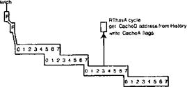
All cache loads require a special cycle, controlled by READTR1, in which they get the correct cache address from History and write the cache flags for the entry being loaded; the data paths of CacheA are used to read this address and write the flags. This RThasA cycle takes priority over all other uses of CacheA and History, and can occur at any time with respect to ADDRESS, which also needs access to these resources. Thus, all control signals sent from ADDRESS are inhibited by RThasA, and any reference in ADDRESS is preempted during this cycle and then resumed. Fig. 9 shows that the RThasA cycle occurs just before the first word of the new block is written into CacheD. (For simplicity and clarity we will not show RThasA cycles in the figures that follow.) During RThasA, the beingLoaded flag is cleared (it was set when the reference was in ADDRESS) and the writeProtected flag is copied from the writeProtected bit in MapRAM (it was passed along from MAP to STORAGE to READTRI). The RThasA cycle is not the logical time to clear beingLoaded, since the block-loading only starts then. It is, however, a convenient time, as the ADDRESS cycle is needed then anyway. No harm results because the cache itself prevents the processor from accessing the new data.
As soon as the transport into CacheD is finished, the word reference that started the miss can be made, much as though it had hit in the first place. If the reference was a fetch, the appropriate word is sent to FetchReg in the processor (and loaded into FetchRegRAM); if a store, the contents of Store-Reg are stored into the new block in the cache.
If the processor tries to use data it has fetched, it is prevented from proceeding, or held until the word reference has occurred (see Section V-A). Each fetch is assigned a sequence number called its tag, which is logically part of the reference: actually it is written into History, and read when needed by READTRI. Tags increase monotonically. The tag of the last fetch started

![]()
![]()

![]()
![]()
![]()
![]() word fetched
word fetched
0 10 1 25 3)
1 1 1 1 1 151 1 1 1 1 1 1 1 15 1 1 1 12°1 1 1 1 1 1 1 1 1 1 1
Fig. 9. A clean miss.
by each task is kept in startedTag (it is written there when the reference is made), and the tag of the last fetch completed by the memory is kept in doneTag (it is written there as the fetch is completed); these are task-specific registers. Since tags are assigned monotonically, and fetches always complete in order within a task, both registers increase monotonically. If started-Tag = doneTag, all the fetches that have been started are done, otherwise not; this condition is therefore sufficient to decide whether the processor should be held when it tries to use FetchReg. Because there is only one FetchReg register per task, it is not useful to start another fetch until the preceding one is done and its word has been retrieved. The tags are therefore used to hold up a fetch until the preceding one is done, and thus can be kept modulo 2, so that one bit suffices to represent a tag. Store references also use the tag mechanism, although this is not logically necessary.
(Instead of a sequence number on each reference, we might have counted the outstanding references for each task. This idea was rejected for the following rather subtle reason. In a single machine cycle three accesses to the counter may be required: the currently running task must read the counter to decide whether a reference is possible, and write back an incremented value; in addition, READTR2 may need to write a decremented value for a different task as a reference completes. Time allows only two references in a single cycle to the RAM in which such task-specific information must be kept. The use of sequence numbers allows the processor to read both startedTag and doneTag from separate RAM's. and then the processor and the memory to independently write the RAM's; thus, four references are made to two RAM's in one cycle, or two to each.)
Other tasks may start references or use data freely while one task has a fetch outstanding. Cache hits, for example, will not be held up, except during the RThasA cycle and while CacheD is busy with the transport. These and other interreference conflicts are discussed in more detail in Section V. Furthermore, the same task may do other references, such as pre-fetches, which are not affected by the tags. The IFU has two FetchReg registers of its own, and can therefore have two fetches outstanding. Hence, it cannot use the standard tag mechanism, and instead implements this function with special hardware of its own.
B. Dirty
Miss
When a
processor or IFU reference misses, and the victim has been changed by a store since arriving in the
cache, a dirty miss has occurred, and the victim must be rewritten in
storage. A dirty miss gives rise to
two storage operations: the write that rewrites
the victim's dirty block from cache to storage, and the read that loads CacheD
with the new block from storage. The actual data transports from and to
the cache are done in this order (as they must
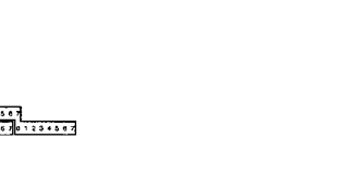
be), but the storage operations are done in reverse order. as illustrated by a fetch with dirty victim in Fig. 10. Thus, as Fig. 10 shows, the victim
reference spends eight cycles in ADDRESS waiting for the fetch to finish with MAP (recall that the asterisks mean no change of
state for the stage). During this time the
victim's transport is done by
WRITETR.
There are several reasons for this arrangement. As we saw in Section III, data transport to and from storage is not done in lockstep with the corresponding storage cycle; only the proper order of events is enforced. The existence of ReadReg and WriteReg permits this. Furthermore, there is a 12-cycle wait between the start of a read in ADDRESS and the latching of the data in ReadReg. These two considerations allow us to interleave the read and victim write operations in the manner shown in Fig. 10. The read is started, and while it proceeds—during the 12-cycle window—the write transport for the victim is done. The data read is latched in ReadReg, and then transported into the cache while the victim data is written into storage.
Doing things this way means that the latency of a miss, from initiation of a fetch to arrival of the data, is the same regardless of whether the victim is dirty. The opposite order is worse for several reasons, notably because the delivery of the new data, which is what holds up the processor, would be delayed by twelve days.
C. Prefetch
and Flush
Prefetch is just like fetch, except that there is no word reference. It is used to preload blocks whose need can be anticipated in advance. Also, because it is treated strictly as a hint, map-fault reporting is suppressed and the tags are not involved, so later references are not delayed. A prefetch that hits, therefore, finishes in ADDRESS without entering MAP. A prefetch that misses will load the referenced block into the cache and cause a dirty victim write if necessary.
A flush explicitly removes the block containing the addressed location from the cache, rewriting it in storage if it is dirty. Flush is used to remove a virtual page's blocks from the cache so that its MapRAM entry can be changed safely, as might be done, for example, when a page is written out to disk. If a flush misses, nothing happens. It it hits, the hit location must be marked vacant, and if it is dirty, the block must be written to storage. To simplify the hardware implementation, this write operation is made to look like a victim write. Since victim writes are provoked only by read operations (such as fetches and prefetches that miss), a dirty flush is converted by

![]()
![]()
![]()
![]()
![]()
![]()
![]()
![]() word
word
fetched
101 1 1 1 151 1111121114 ri 1 1
1 ri 1 1 1151 1 1 1 1 D1 1 1 1 1351 1 1 1 roi
Fig.
10. A dirty miss.
the hardware into a flushFetch reference, which is treated
almost exactly like a prefetch. When a flush in ADDRESS hits, three
things happen:
1) the victim for the selected row of CacheA is changed to point
to the hit column;
2) the
vacant flag is set;
3) if the dirty flag for that column is set, the flush is
converted into a flushFetch.
Proceeding like a prefetch, the flushFetch does
a useless read (which is harmless because
the vacant flag has been set), and then a
write of the dirty victim. Fig. 11 shows a dirty flush. The flushFetch spends two cycles in ADDRESS instead of the usual one because
of an uninteresting implementation problem.
D. Dirty I/Oread
If an I/Oread reference
hits in a column with dirty set, the data must come from the cache rather than
from storage. This is made as similar as possible to a clean I/Oread, since
otherwise the bus scheduling would be drastically
different. Hence, a full storage read is
done, but at the last minute data from the cache
are put on FastOutBus in place of the data coming from storage, which are ignored. Fig. 12 illustrates a dirty
I/Oread followed by two clean ones. Note that CacheD is
active at the same time as for a standard
read, but that it is unloaded rather than
loaded. This simplifies the scheduling of CacheD, at the expense
of tying up FastOutBus for one extra cycle. Since many operations use CacheD, but only I/Oread uses FastOutBus, this is a worthwhile simplification (see
Section V-C).
V. TRAFFIC CONTROL
Thus far we have considered
memory operations only in isolation from each other. Because the system is
pipelined, however, several different operations can be active at once. Measures must be taken to prevent concurrent references
from interfering with each other, and to prevent new operations from starting if the system is not ready to accept them. In
this section we discuss those measures.
Table IV lists the
resources used by each pipeline stage in three
categories: private resources, which are used only by one stage; handoff
resources, which are passed from one stage to another in an orderly way guaranteed not to result in
conflicts;

![]()
![]()
![]()
![]()
![]() Thia is ignored
bocaus•
Thia is ignored
bocaus•
the vecoM flag 13 8@f
0 5 10 15 20 25 30 35 40
I 1 1111111111111111111111111111111
1 1 i
1 11111
Fig. 11. A dirty flush.
and complex resources, which are shared among several stages in ways
that may conflict with each other. These conflicts are resolved
in three ways.
1) If
the memory system cannot accept a new reference from the processor, it rejects it, and notifies the processor by asserting
the Hold signal.
2) A reference. once started, waits in ADDRESS until its immediate
resource requirements (i.e., those it needs in the very next cycle) can be met: it then proceeds to MAP or
to HITDATA, as shown in Fig. 3.
3) All remaining conflicts are dealt with in a
single state of the MAP stage.
We will consider the three methods in turn.
A. Hold
Hold is the signal generated by the memory
system in response to a processor request that cannot yet be satisfied. Its effect is to convert the microinstruction containing the
request into a jump-to-self; one cycle is thus lost. As
long as the same task is running in the
processor and the condition causing Hold is
still present, that instruction will be held repeatedly. However, the processor may switch to a higher priority task
which can perhaps make more progress.
There are four reasons for the memory system to
generate Hold.
1)
Data Requested Before It is Ready: Probably
the most common type of Hold occurs after a
fetch, when the data are requested
before they have arrived in FetchReg. For a hit that is not delayed in ADDRESS (see below), Hold only happens if the
data are used early in the very next cycle (i.e., if the instruction after the fetch sends the data to the
processor's ALU rather than just
into a register). If the data are used late in the next cycle they
bypass FetchReg and come directly from CacheD
(Section WC); if they are used in any later cycle they come frorh FetchReg. In
either case there will be no Hold. If the
fetch misses, however, the matching FetchReg operation will be held (by the tag mechanism) until the
missing block has been loaded into
the cache, and the required word fetched into FetchReg.
2)
ADDRESS BUSY: A
reference can be held up in ADDRESS for a
variety of reasons, e.g., because it must proceed to
MAP, and MAP is busy with a previous
reference. Other reasons are discussed in
Section V-B below. Every reference
|
RT 1 I |
RT2 |
PT/ 1 RT2 |
RT1 I RT2 |
|
dirty |
i/Oreau |
clean 1/Oread 1 |
clean I/Oread 2 |
Fig. 12. A dirty I/Oread and two clean ones.
TABLE IV
PIPELINE
RESOURCES
|
|
PROC |
ADDRESS |
f IITDATA |
MAP |
WRII1ITR |
STORAGE |
READTR I |
REA DTR2 |
|
Pd.!,
Resource |
|
|
|
MapR AM |
WntcOus &Ge, Tod
n Bus |
Sumas:RAN( |
|
|
|
Hasioli
Resosraes |
|
|
|
|
Y. -.Res |
WnieRes ReadRes |
R :saes Rea
dBus EcCor FamOur.Bus |
RcadBus
li:Cor FastOutBus |
|
Coopka
Rescumces |
Fach
R es SLoreRes Hume) |
CarleA f
I 'gory |
FettehRes Swats C.:1*D |
Iiisuary |
Cachet) |
|
CachcA CadleD History |
Fetchlt el StoreRes
Cachet) I kaary |
needs
to spend at least one cycle in ADDRESS, so new references will be held as long as ADDRESS is
busy. A reference needs the data paths of CacheA in order to load
its address into ADDRESS,
and these are busy during the RThasA cycle discussed
above (Section IV-A); hence a reference in the cycle before
RThasA is held.
3) StoreReg Busy: When a store
enters ADDRESS, the
data supplied by the processor is loaded into StoreReg. If the
store hits and there is no conflict for CacheD. StoreReg is
written into CacheD in the next cycle. as Fig. 4 shows. If it misses, StoreReg
must be maintained until the missing block arrives in
CacheD, and so new stores must be held during this time because
StoreReg is not task-specific. Even on a hit. CacheD may
be busy with another operation. Of course new stores by the
same task would be held by the tag mechanism anyway, so StoreReg busy
will only hold a store in other tasks. A task-specific StoreReg would have
prevented this kind of Hold, but the
hardware implementation was too expensive to do this, and we observed that stores are rare compared to
fetches in any case. (Performance
measurements reported in Section VII support
this.)
4) History Busy: As discussed in
Section III-C, a reference uses various parts of the History memory at
various times as it makes it way through the pipeline.
Microinstructions for reading History are provided, and they must be held if they will conflict with any other use.
The memory system must generate Hold for precisely
the
above
reasons. It turns out, however, that there are several situations
in which hardware can be saved or the microcycle time reduced if
Hold is generated when it is not strictly needed. This
was done only in cases that we expect to occur rarely, so the
performance penalty of the extra Holds should be small. An extra Hold has no
logical effect, since it only converts the current
microinstruction into a jump-to-self. One example of this situation is that a reference in the cycle
after a miss is always held, even
though it must be held only if the miss' victim is dirty or the map is
busy; the reason is that the miss itself is detected
barely in time to generate Hold, and there is no time for additional logic. Another example: uses of
FetchReg are held while ADDRESS is
busy, although they need not be. since they do not use it.
B. Waiting in ADDRESS
A reference in ADDRESS normally proceeds either
to HITDATA (in
the case of a hit) or to MAP (for a miss, a victim write or an I/0
reference) after one cycle. If HITDATA or MAP is busy, it will wait in ADDRESS, causing
subsequent references to be held because ADDRESS is busy, as discussed
above.
HITDATA uses
CacheD, and therefore cannot be started when CacheD is busy. A
reference that hits must therefore wait in ADDRESS while
CacheD is busy, i.e., during transports to and from storage,
and during single-word transfers resulting from previous
fetches and stores. Some additional hardware would have
enabled a reference to be passed to HITDATA and wait
there, instead of in ADDRESS.
for CacheD to become free; ADDRESS would then be free to accept another reference. This performance
improvement was judged not worth the requisite hardware.
When MAP is busy with an earlier
reference, a reference in ADDRESS will wait if it needs MAP. An example of this
is shown in Fig. 10, where the victim write waits while MAP handles the read.
However, even if MAP is
free, a write must wait in ADDRESS until it can start WRITETR; since
WRITETR always takes
longer than MAP, there
is no point in starting MAP first, and the implementation is simplified by the rule
that starting MAP always frees ADDRESS. Fig. 13 shows two
IDIIII151IIIICII11151t11~fI1IP1111PII1I11III
'I1 Fig. 13. Two 1/0writes.
back-to-back
I/Owrites, the second of which waits one extra cycle in ADDRESS before starting both WRITETR
and MAP.
The last reason for waiting in ADDRESS has to do with the beingLoaded flag in the cache. If ADDRESS finds that being-Loaded is set anywhere in the row it touches, it waits until the flag is cleared (this is done by READTR I during the RThasA cycle). A better implementation would wait only if the flag is set in the column in which it hits, but this was too slow and would require special logic to ensure that an entry being loaded is not chosen as a victim. Of course it would be much better to Hold a reference to a row being loaded before it gets into ADDRESS, but unfortunately the reference must be in ADDRESS to read the flags in the first place.
C Waiting
in MAP
The traffic control techniques discussed thus far, namely, Hold and waiting in ADDRESS, are not sufficient to prevent all the conflicts shown in Table IV. In particular, neither deals with conflicts downstream in the pipeline. Such conflicts could be resolved by delaying a reference in ADDRESS until it was certain that no further conflicts with earlier references could occur. This is not a good idea because references that hit, which is to say most references, must be held when ADDRESS is busy. If conflicts are resolved in MAP or later. hits can proceed unimpeded, since they do not use later sections of the pipeline.
At the other extreme, the rule could be that a stage waits only if it cannot acquire the resources it will need in the very next cycle. This would be quite feasible for our system, and the proper choice of priorities for the various stages can clearly prevent deadlock. However, each stage that may be forced to wait requires logic for detecting this situation, and the cost of this logic is significant. Furthermore, in a long pipeline gathering all the information and calculating which stages can proceed can take a long time, especially since in general each stage's decision depends on the decision made by the next one in the pipe.
For these reasons we adopted a different strategy
in the Dorado. There is one point,
early in the pipeline but after ADDRESS, at which all remaining
conflicts are resolved. A reference
is not allowed to proceed beyond that point without a guarantee that no
conflicts with earlier references will occur; thus
no later stage ever needs to wait. The point used for this purpose is state 3 of the MAP stage, written as MAP.3. No shared resources are used in states 0-3, and STORAGE is not started until state 4. Because there is just one wait state in the pipeline, the exact
timing of resource demands by later stages is
known and can be used to decide whether conflicts are possible. Davidson's
technique [4] might have been used to control the MAP wait, but it is too expensive in hardware.
The actual implementation uses a combinational function of signals from other pipeline stages to decide whether to repeat
MAP.3 or not. ‑
We will now discuss in turn the various conflicts that lead to waiting in MAP.3.
Synchronizing STORAGE and WRITETR: In a write operation WRITETR runs in parallel but not in lockstep with MAP; see, for example, Fig. 10. Synchronization of the data transport with the storage reference itself is accomplished by two things.
MAP.3 waits for WRITETR to signal that the transport is far enough along that the data will arrive at the Storage-RAM chips no later than the write signal generated by STORAGE. This condition must be met for correct functioning of the chips. Fig. 13 shows MAP waiting during an I/Owrite.
WRITETR will wait in its next-to-last state for STORAGE to signal that the data hold time of the chips with
respect to the write signal has
elapsed; again, the chips will not work
if the data in WriteReg is changed before this point. Fig. 10 shows WRITETR waiting
during a victim write. The wait shown
in the figure is actually more conservative than it needs to be. since WRITETR does not
change WriteReg immediately when it
is started.
CacheD:
Consecutive Cache Loads: Loading
a block into CacheD takes 9 cycles,
as explained in Section IV-A, and a word
reference takes one more. Therefore, although the pipeline stages proper are 8 cycles long, cache
loads must be spaced either 9 or 10 cycles apart to avoid conflict in CacheD. After a fetch or store, the next cache
load must wait 10 cycles, since these references tie up CacheD for 10
cycles. After a prefetch, flush Fetch or
dirty I/Oread, the next cache load
must wait for 9 cycles. STORAGE sends MAP a signal that
causes MAP.3 CO %%, ait
for one or two extra cycles, as appro‑
priate. Fig. 14 shows a fetch followed by a prefetch, followed by a store, and illustrates how CacheD conflict is avoided by extra cycles spent in MAP.3. Note that the prefetch waits two extra cycles, while the store only waits one extra.
CacheD: Load and Unload: The other source of conflict for CacheD is between loading it in a miss read and unloading it in a victim write. This conflict does not arise between a miss read and its own victim because the victim is finished with CacheD before the read needs it; Fig. l0 illustrates this. There is a potential conflict, however, between a miss read and the next reference's victim. CacheD is loaded quite late in a read, but unloaded quite early in a write, as the figure shows, so the pipeline by itself will not prevent a conflict. Instead, the following interlock is used. If a miss is followed by another miss with a dirty victim:
ADDRESS waits to start WRITETR for the victim transport until the danger of CacheD conflict with the first miss is past.
MAP.3 waits while processing the read for the second miss (not its victim write) until WRITETR has been started.
|
RT1 1 |
RT2 |
RT1 1 |
RT2 |
RT1 1 |
RT2 |
|
retch |
loading i |
pretetch |
loading |
store |
load-ng II |
word word
fetched shed
0 5 10 15 20 25 35 40 45
![]() Fig. 14. Cache
load conflict for CacheD.
Fig. 14. Cache
load conflict for CacheD.
store fetch fetch's
dirty victim
![]()

![]()
![]()
![]()
![]()
![]()
![]()
![]()
![]()
![]()
![]()
![]()
![]()
![]() PROC ADDRESS WRITETR MAP STORAGE READTR1 READTR2
PROC ADDRESS WRITETR MAP STORAGE READTR1 READTR2
10 1 2 3 4 5 6
![]() 0 1 2 3 4 5 6_
1
0 1 2 3 4 5 6_
1
10___ 1 2 3 4 5 8 1
7101 2 3 4 5 6
![]() 0 1 2 3 4 5 6
71L3 1 2 3 4 5 8 1
0 1 2 3 4 5 6
71L3 1 2 3 4 5 8 1
101 234 5 6_122 2 3 4 5 8 71
![]()
![]()
![]()
![]()
![]()
![]()
wad word
stored fetched
10 15 20 25 33 35 ao as so ss
101111151 I 1 1 1 I I 1 1 I 1 I I I I
1 1 I 1 I I
I 1 I 1 I 1 I I I I 1 i 1 I 1 I I 1 I 1 1 1
I1
Fig. 15. Cache
load/unload conflict for CacheD.
This ensures that the second read will not get ahead of
its victim write enough to cause a CacheD conflict. Actually,
to save hardware we used the same signal to control both waits, which causes
MAP.3 to wait two cycles longer than necessary.
Fig. 15 shows a store with clean victim followed
by a fetch with
dirty victim and illustrates this interlock. ADDRESS waits until cycle 26 to start WRITETR. Also,
the fetch waits in MAP.3 until the same cycle, thus spending 13 extra cycles there. which forces the fetch victim to spend 13 extra cycles in
ADDRESS. The two-cycle gap in
the use of CacheD shows that the fetch could have left MAP,3 in cycle 24.
FastOutBus Conflicts: The
final reason for waiting in MAP.3 is a conflict over the FastOutBus, used by
I/Oread references. A dirty I/Oread uses
FastOutBus one cycle later than an
ordinary I/Oread, so that it can use CacheD with the same timing as a cache load; see Section IV-D. The
potential FastOutBus conflict is prevented by delaying an I/Oread immediately after a dirty I/Oread by one extra
cycle in MAP.3. Fig. 12 illustrates this, and also shows how clean 1/Oreads can
start every eight cycles and encounter
no delay.
VI. PHYSICAL IMPLEMENTATION
A primary design goal of the Dorado as a personal computer
is
compactness. The whole machine (except the storage) is implemented on a single type of logic board, which is 14 in square, and can hold 288 16-pin integrated
circuits and 144 8-pin packages
containing terminating resistors. There are 192 pins on each side of the board; 8 are used for power connections,
and the remainder in pairs for grounds and signals. Thus, 184 signals can enter or leave the board. Fig. 16
shows a Dorado board.
Boards slide into zero-insertion-force
connectors mounted in two sideplanes, one on each side of the board,
which have both bus wiring and interboard point-to-point wiring. Inter-board spacing is
0.625 in, so that the chassis stack of 24 board slots is 15 in high. The entire machine, including cooling and power,
occupies about 4.5 cubic feet. Fig. 17 shows a Dorado chassis atop its power
supply cabinet. For the office or laboratory
environment this comparatively small assembly slides into a soundproofing enclosure that measures four
feet X four feet X two feet. Fig. 18
shows a Dorado in its enclosure, which includes room for a Trident disk.
Dorados can also be rack-mounted.
Fig. 17. Dorado chassis and power supply.
Main storage boards are the same size as logic
boards, but are designed to hold an array of MOS RAM's instead of random ECL
logic. A pair of storage boards make up a module, which holds 512K bytes (plus error correction) when
populated with 16K RAM's, 2M bytes with 64K RAM's, or 8M bytes with
(hypothetical) 256K RAM's. There is room for four modules, and space not used for storage modules can hold I/O boards. Within a module, one board stores all the
words with even addresses, the other
those with odd addresses. The boards are identical, and are
differentiated by sideplane wiring.
A standard Dorado contains, in addition
to its storage boards, 11 logic boards,
including disk, display, and network controllers. Extra board positions can
hold additional I/O controllers. Three boards implement the memory system (in
Fig. 18. Dorado in enclosure_
about
800 chips); they are called the Address board, the Pipe board, and the Data board, names which reflect
the functional partition of the
system. The Address board contains the processor interface, base registers and
virtual address computation, CacheA (implemented
in 256 by 4 RAM's) and its comparators, and
the lru computation. It also generates Hold, addresses the Data board on hits, and sends storage references to
the Pipe board.
The
Data board houses CacheD, which is implemented with 1K by I or 4K by 1 ECL RAM's, and holds 8K or
32K bytes, respectively. This board is also the source for FastOutBus and WriteBus. and the sink for FastlnBus and ReadBus, and it holds the Hamming code generator, checker, and
corrector. This Pipe board implements MapRAM, all of the pipeline stage automata (except ADDRESS and HITDATA) and their interlocks, and the fault reporting. destination bookkeeping, and refresh control for the MapRAM and
StorageRAM chips. The
History memory is distributed across the boards: addresses on the Address board, control information on
the Pipe board, and data errors on the Data
board.
Although
our several prototype Dorados can run at a 50 ns microcycle, additional machines will run instead at 60
ns. This is due mainly to a change
in board technology from a relatively expensive point-to-point wire-routing
method to a cheaper Manhattan routing method.
VII. PERFORMANCE
The
memory system's performance is best characterized by two key quantities: the cache hit rate and the
percentage of cycles lost due to
Hold (Section V-A). In fact, Hold by itself measures
the cache hit rate indirectly, since misses usually cause many cycles of Hold. Also interesting are the frequencies of
stores and of dirty victim writes, which affect performance
TABLE V
MEMORY SYSTEM PERFORMANCE
|
|
As a percentage
nfcyclest References Ilolds |
As a
percentage of sere:racer tins Stores |
As a percentage
of raises: tains |
||
|
Beads |
36.4 |
8.14 |
99.27 |
10.5 |
16.3 |
|
Placer |
42.9 |
4.89 |
99.82 |
13.7 |
65.5 |
|
TEX |
38.4 |
6.33 |
9955 |
15.2 |
34.9 |
by increasing the number of Holds and by consuming storage bandwidth. We measured these quantities with hardware event-counters, together with a small amount of microcode that runs very rarely and makes no memory references itself. The measurement process, therefore, perturbs the measured programs only trivially.
We measured three Mesa programs: two VLSI design-automation programs, called Beads and Placer, and an implementation of Knuth's TEX [10]. All three were run for several minutes (several billion Dorado cycles). The cache size was 4K 16-bit words.
Table V shows
the results. The first column shows the percentage of cycles that contained cache references (by either the
processor or the i
Fu), and the second, how many cycles were
lost because they were held. Holds, happily, are fairly rare_ The hit rates
shown in column three are gratifyingly large—all
over 99 percent. This is one reason that the number of held cycles is small: a miss can cause the
processor to be held for about 30
cycles while a reference completes. In fact, the table shows that Hold
and hit are inversely related over the programs
measured. Beads has the lowest hit rate and the most Holds; Placer has the highest hit rate and the
fewest Holds.
The percentage of
store references is interesting because stores eventually give rise to dirty
victim write operations, which
consume storage bandwidth and cause extra Holds by tying up the ADDRESS section
of the pipeline. Furthermore, one of the reasons that the StoreReg register was
not made task-specific was the
assumption that stores would be relatively rare (see the discussion of StoreReg in Section V-A). Table
V shows that stores accounted for
between 10 and 19 percent of all
references to the cache.
Comparing the
number of hits to the number of stores shows that the write-back discipline used in the cache was a good choice.
Even if every miss had a dirty victim, the number of victim writes would still be much less than under
the write-through discipline, when
every store would cause a write. In fact,
not all misses have dirty victims, as shown in the last column of the table. The percentage of misses with
dirty victims varies widely from
program to program. Placer, which had
the highest frequency of stores and the lowest frequency of misses, naturally has the highest frequency of
dirty victims. Beads, with the most
misses but the fewest stores, has the lowest.
The last three columns of the table show that considering the three programs together. write operations
would increase about a hundredfold if write-through were used instead of write-back. Total storage operations not
due to fast 1/0 would increase by a
factor of about 25.
ACKNOWLEDGMENT
The concept and structure of the Dorado memory system are due to B. Lampson and C. Thacker. Much of the design was brought to the register-transfer level by Lampson and B.
'so can r;-„I ri ete.te ; err.] ottretaart tn ;net nr A taro,.
done by the authors and E. McCreight,
who was responsible for the main storage boards. Debugging software and microcode were written by E. Fiala. W.-S. Haugeland, and
G. McDaniel. Haugeland and McDaniel
were also of great help in collecting
the statistics reported in Section VII. Useful comments on earlier versions of this paper were contributed by F.
Baskett, E. Cohen, G. McDaniel, J. Morris, T. Rentsch, C. Thacker, and the referees.
REFERENCES
[1]
J. Bell, D. Casasent, and C. G. Bell, "An investigation of
alternative cache organizations," IEEE Trans.
Comput., vol.
C-23, pp. 346-351, Apr. 1974.
[2]
L. Bloom, M. Cohen, and S. Porter, "Considerations in the design of
a computer with high
logic-to-memory speed ratio," in Proc.
Gigacycle Comput. Syst., A IEE Special Pub. S-136, Jan. 1962, pp. 53-63.
[3] C. J. Conti. "Concepts for buffer storage," IEEE Comput. Group News, vol.
2, pp. 9-13, Mar. 1969.
14] E. S. Davidson, "The design and control of pipelined function
generators," in Proc. 197!
Int. Conf Syst. Networks, Comput., Oaxtepec,
Mexico, Jan. 1971, pp. 19-21.
[5]
L. P. Deutsch, "Experience with a microprogrammed Interlisp
system," in Proc. 11th
Annu. Microprogramming Workshop, Asilomar
Conf. Ground, Pacific Grove, CA, Nov. 1978.
[6] J. W. Forgie, "The Lincoln
TX-2 input-output system," in Proc.
Western Joint Comput. Conf., Los Angeles, CA, Feb. 1957, pp. 156- 160.
[7]
C. M. Geschke, J. H. Morris, Jr., and E. H. Satterthwaite, "Early
experience with
Mesa," Commun. Ass. Comput. Mach., vol. 20, pp. 540-552, Aug. 1977.
[8]
D. Ingalls,
"The Smalltalk-76 programming system: Design and implementation," in Proc. 5th ACM Symp. Principles of Programming Lang., Tucson, AZ, Jan. 1978, pp. 9-16.
[9] K. R. Kaplan and R. 0. Winder,
"Cache-based computer systems," Computer,
pp. 30-36, Mar.
1973.
[10] D. E. Knuth, TEX and METAFONT: New Directions in Typesetting. Bedford, MA: American Math. Soc.
and Digital Press, 1979.
[11] B. W. Lampson, G. A. McDaniel, and S. M. Ornstein, "An
instruction fetch unit for a high
performance personal computer," Xerox Palo Alto Res. Cen., Palo Alto, CA,
Tech. Rep. CSL-81-1, 1981.
[121 B. W. Lampson and K. A. Pier, "A processor for a high
performance personal
computer," in Proc. 7th Int. Symp. Comput.
Arch., La Baule,
France, May 1980, pp.
146-160; also in Tech. Rep. CSL-81-1, Xerox Palo
Alto Res. Cen., Palo Alto, CA, 1981.
[13] J. S. Liptay, "Structural
aspects of the System/360 model 85. H. The cache," IBM Syst. J., vol. 7, no. I, pp. 15-21,1968.
[14] R. M. Metcalfe and D. R. Boggs,
"Ethernet: Distributed packet switching for local computer networks," Commun. Ass. Comput. Mach., vol.
19, pp. 395-404, July 1976.
[15] J. G. Mitchell, W. Maybury, and R.
Sweet, Mesa Language Manual, Xerox Palo Alto Res. Cen., Palo
Alto, CA, Tech. Rep. CSL-79-3, 1979.
[16] A. Pohm, 0. Agrawal, and R. Monroe,
"The cost and performance tradeoffs of buffered memories," Proc.
IEEE, vol. 63, pp. 1129-1135, Aug.
1975.
[17] M. D. Schroeder, "Performance
of the GE-645 associative memory while MULTICS is in operation," in Proc. ACM SIGOPS Workshop Syst. Performance Evaluation, Harvard Univ., Cambridge, MA, Apr. 1971, pp. 227-245.
[18] W. D. Strecker, "Cache
memories for PDP-1 I family computers," in Proc. 3rd
Annu. Symp. Compel. Arch., 1976, pp.
155-158.
[19] A. S. Tanenbaum, "Implications
of structured programming for machine architecture," Commun.
Ass. Comput. Mach., vol. 21, pp. 237-246, Mar. 1978.
[20] W. Teitelman, Interlisp Reference Manual. Palo Alto, CA: Xerox Palo
Alto Res. Cen., 1978.
[21] C. P. Thacker, E. M. McCreight, B.
W. Lampson, R. F. Sproul', and D. R. Boggs, "Alto: A personal computer," in Computer Structures: Readings and
Examples, 2nd ed.,
Siewiorek, Bell, and Newell, Eds. New York: McGraw-Hill, 1981, to be published;
also in Tech. Rep. CSL-79-11, Xerox Palo
Alto Res. Cen., Palo Alto, CA, 1979.
[22] R. M. Tomasulo, "An efficient
algorithm for exploiting multiple arithmetic units," IBM J. Res. Develop., vol. 11, pp. 25-33, Jan. 1967.
[23] M. V. Wilkes, "Slave
memories and segmentation," IEEE Trans.
........ CIA 4,0 I


 Douglas W. Clark received the B.S. degree in engineering and applied science from
Yale University, New Haven, CT, in 1972 and the Ph.D. degree in computer science from
Carnegie-Mellon University, Pittsburgh,
PA, in 1976.
Douglas W. Clark received the B.S. degree in engineering and applied science from
Yale University, New Haven, CT, in 1972 and the Ph.D. degree in computer science from
Carnegie-Mellon University, Pittsburgh,
PA, in 1976.
From 1976 to
1980 he was a Member of the Research Staff at the Xerox Palo Alto Research Center, Palo Alto, CA, where he worked mainly on the design and implementation of the Dorado computer. In 1980 he joined the Systems Architecture
Group of the Digital Equipment Corporation, Tewksbury, MA, as a
Principal Engineer. His current work is in the areas of computer architecture and hardware performance measurement and evaluation.


 Kenneth A. Pier received the B.S. degree in 1968 and the M.S. degree in 1975 from
the University of California, Berkeley.
Kenneth A. Pier received the B.S. degree in 1968 and the M.S. degree in 1975 from
the University of California, Berkeley.
Since 1977 he has been a Member of the Research Staff at the Xerox Palo Alto Research Center, Palo Alto, CA. Until 1980 he
worked primarily on
the design, implementation, and commissioning of the Dorado system. In 1980 he
joined the Imaging
Sciences Laboratory at Xerox and is now working in the area of computer graphics and imaging systems.
Congestion Control of Packet Communication
Networks
by Input Buffer Limits A Simulation
Study
SIMON S. LAM, SENIOR MEMBER,
IEEE, AND Y. C. LUKE LIEN, STUDENT MEMBER.
IEEE
Abstract—An
experimental study was conducted using a network simulator to investigate the performance of packet communication networks
as a function of: the network resource capacities (channels, buffers), the network load (number of virtual
channels, virtual channel loads),
protocols (flow control, congestion control, routing), and protocol parameters (virtual channel window size,
input buffer limits). Performance characteristics are shown and the design of
input buffer limits for
network congestion control, virtual
channel window size, and nodal
buffer capacity addressed. Network design strategies for the control of load fluctuations are proposed and discussed.
Index Terms—Buffer management, congestion control, flow control, input buffer limits, packet switching networks,
performance analysis, resource allocation, store-and-forward
networks.
Manuscript received December 30, 1980;
revised May 5, 1981. This work was supported
by the National Science Foundation under Grant ECS78- 01803. A short
version of this paper was presented at the International Conference on Computer Communications, Atlanta, GA,
October 1980.
S. S. Lam is with the
Department of Computer Sciences, University of Texas, Austin, TX 78712.
Y. C. L. Lien was with the Department of Computer Sciences, University of Texas, Austin, TX 78712. He is
now with the IBM T. J. Watson Research Center, Yorktown Heights, NY 10598.
I. INTRODUCTION
HE
OBJECTIVE of a packet communication network
is to
reliably deliver packets from their sources to their destinations within acceptable time delays.
Thus, an important performance
measure of a packet network is its throughput rate
in packets delivered per second.
Throughput
is generated when individual packets progress through the network following unite
(preferably acyclic) paths. Packets
admitted into the network require the allocation of different types of
resources to progress. The packet buffers at a network node form one type of resource. There are
different types of buffer
resources corresponding to different nodes in the network. The set of communication channels (usually
just one) that transports
packets from one node to another node is another type of resource. There are different types of channel resources corresponding to different communication
links.
To generate a packet's worth of throughput, the network must first admit a packet and then allocate to
it a set of re‑
• I'. • n-n • • ..... r CN • • •-•