A Processor for a High-Performance Personal Computer
Butler W. Lampson and Kenneth A. Pier
Xerox Research Center
3333 Coyote Hill Road
Palo Alto, California 94304
This document was produced from a Word original. There may
be problems with the formatting. To see the intended form, follow one of the following
links: Acrobat as published, Acrobat (from Word), Word
Appeared in Proc. 7th IEEE Symposium on Computer Architecture, La Baule, France, 1980, pp 146-160. Reprinted in 25 years of the International Symposia on Computer Architecture (selected papers), 1998, pp 180-194. Also in Technical Report CSL-81-1, Xerox Palo Alto Research Center.
This document was produced from the published original by
scanning and OCR. There may be errors.
CH1494-4/80/0000-0146 $00.75 © 1980 IEEE, 146-160
This paper describes the design goals, micro-architecture, and implementation of the microprogrammed processor for a compact high performance personal computer. This computer supports a range of high level language environments and high bandwidth I/O devices. Besides the processor, it has a cache, a memory map, main storage, and an instruction fetch unit; these are described in other papers. The processor can be shared among 16 microcoded tasks, performing microcode context switches on demand with essentially no overhead. Conditional branches are done without any lookahead or delay. Microinstructions are fairly tightly encoded, and use an interesting variant on control field sharing. The processor implements a large number of internal registers, hardware stacks, a cyclic shifter/masker, and an arithmetic/logic unit, together with external data paths for instruction fetching, memory interface, and I/O, in a compact, pipelined organization.
The machine has a 50 ns microcycle, and can execute a simple macroinstruction in one cycle; the available I/O bandwidth is 640 Mbits/sec. The entire machine, including disk, display and network interfaces, is implemented with approximately 3000 MSI components, mostly ECL 10K; the processor is about 35% of this. In addition there are up to 4 storage modules, each with about 300 16K or 64K RAMs and 200 MSI components, for a total of 8 Mbytes. Several prototypes are currently running.
1. Introduction
The machine described in this paper, called the Dorado, was designed by and for the Computer Science Laboratory (CSL) of the Xerox Palo Alto Research Center. CSL has approximately forty people doing research in most areas of computer science, including VLSI design, communications, programming systems, graphics and imaging, office automation, artificial intelligence, computational linguistics, and analysis of algorithms. There is a heavy emphasis on building usable prototype systems, and many such systems, both hardware and software, have been developed over the last seven years. Most are part of a personal computing environment which is loosely coupled to other such environments, and to service facilities for storage and printing, by a high bandwidth communication network [8]. .
The Dorado is intended to provide the hardware base for the next generation of system research in CSL. Earlier machines have limitations on virtual address size, real memory size, memory bandwidth, and processor speed that severely hamper our work. The size and speed of the Dorado minimize these limitations.
The paper has seven sections. We begin by sketching the history of the machine’s development (§ 2). Then we discuss the design goals for the Dorado (§ 3), and explain how these goals and the available technology determine the high level processor architecture (§ 4). Next, we present the most important details of the processor architecture (§ 5) and some interesting aspects of the implementation (§ 6). Final sections describe the machine’s performance and status (§ 7 and 8).
2. History
The Dorado is a descendant of a small personal computer called the Alto, which was designed and built as an experimental machine in CSL during 1973 [8]. The Alto was a fairly simple machine, but it had several features which turned out to be important:
• a microprogrammed processor that is efficiently shared among all the device controllers as well as the virtual machine interpreter;
• a fairly high resolution display system that uses a full bitmap resident in the Alto main memory;
• a device for pointing at images on the display;
• an interface to a high bandwidth communication network.
The microarchitecture allows all the device controllers to share the full power of the processor, rather than having independent access to the memory. As a result, controllers can be small, and yet the I/O interface provided to programs can be powerful. This concept of processor sharing is fundamental to the Dorado as well, and is more fully explained in Section 4.
Although there are now hundreds of Altos at work within Xerox, and in early 1980 they still form the hardware base for CSL, it was clear by 1976 that a large and rapidly increasing amount of effort was going into surmounting the Alto’s limitations of space and speed, rather than trying out research ideas in experimental systems. CSL therefore began to design a new machine aimed at relieving these burdens. During 1976 and 1977, design work on the Dorado proceeded in CSL and the System Development Department. Requirements and contributions from parts of Xerox outside of CSL affected the design considerably, as did the tendency toward grandiosity well known in follow-on systems. The memory bandwidth and processor throughput were substantially increased.
In 1977, implementation of the laboratory prototype for the Dorado began. The prototype packaging and a design automation system had already been implemented, and were used for constructing and debugging Dorado Model 0. A small team of people worked steadily on all aspects of the Dorado system until summer of 1978, when the prototype successfully ran all the Alto software. During the summer and fall of 1978 we used the lessons learned in debugging and microcoding the Model 0, together with the significant improvements in memory technology since the Model 0 design was frozen, to redesign and reimplement nearly every section of the Dorado. We fixed some serious design errors and a number of annoyances to the microcoder, substantially expanded all the memories of the machine, and speeded up the basic cycle time. Dorado Model 1 came up in the spring of 1979.
3. Goals
This section of the paper describes the overall design goals for the Dorado. The high level architecture of the processor, described in the next section, follows from these goals and the characteristics of the available technology.
The Dorado is intended to be a powerful but personal computing system. It supports a single user within a programming system which may extend from the microinstruction level to a fully integrated programming environment for a high-level language; programming at all levels must be relatively easy. The machine must be physically small and quiet enough to occupy space near its users in an office or laboratory setting, and inexpensive enough to be acquired in considerable numbers. These constraints on size, noise, and cost have a major effect on the design.
In order for the Dorado to quickly become useful in the existing CSL environment, it must be compatible with the Alto software base. High-performance Alto emulation is not a requirement, however; since the existing software is also obsolescent and due to be replaced, the Dorado only needs to run it somewhat faster than the Alto can.
Instead, the Dorado is optimized for the execution of languages that are compiled into a stream of byte codes; this execution is called emulation. Such byte code compilers exist for Mesa [3, 6], Interlisp [2, 7] and Smalltalk [4]. An instruction fetch unit (IFU) in the Dorado fetches bytes from such a stream, decodes them as instructions and operands, and provides the necessary control and data information to the processor; it is described in another paper [5]. Further support for this goal comes from a very fast microcycle, and a processor powerful enough to handle a simple macroinstruction in a single microinstruction. There is also a cache which has a latency of two cycles, and can deliver a word every cycle. The goal of fast execution affects the choices of implementation technology, microstore organization, and pipeline organization. It also mandates a number of specific features, for example, stacks built with high speed memory, and hardware base registers for addressing software contexts.
Another major goal for the Dorado is to support high-bandwidth input/output. In particular, color monitors, raster scanned printers, and high speed communications are all part of the research activities within CSL; one of these devices typically has a bandwidth of 20 to 400 Mbits/second. Fast devices should not slow down the emulator too much, even though the two functions compete for many of the same resources. Relatively slow devices must also be supported, without tying up the high bandwidth I/O system. These considerations clearly suggest that I/O activity and emulation should proceed in parallel as much as possible. Also, it must be possible to integrate as yet undefined device controllers into the Dorado system in a relatively straightforward way. The memory system supports these requirements by allowing cache accesses and main storage references to proceed in parallel, and by fully segmented pipelining which allows a cache reference to start in every cycle, and a storage.reference to start in every storage cycle; this system is described in another paper [1].
Any system for experimental research should provide adequate resources at many levels. For the processor,.this means plenty of high speed internal storage as well as ample speed. Hardware support for handling arbitrary bit strings, both large and small, is also necessary.
4. High level architecture
We now proceed to consider the major design decisions which shaped the Dorado processor. For the most part these were guided by the goals set out above, the available implementation technology, and our past experience. In this section we stay at a high level, reserving the details of the architecture for the next
The Dorado fits into a very compact package, illustrated in figure la; a high-level block diagram is shown in figure Ib. Circuits are mounted on large, high density logic boards (288 logic packages/board). The boards slide horizontally into zero-insertion-force connectors mounted in dual backpanels (“sidepanels”); they are .625 inches apart. This density makes it possible to reconcile the goals of size and capability. Certain sacrifices are made, however. For example, it is not possible to access every signal with a scope probe for debugging and maintenance. We make up for this by providing sophisticated debugging facilities, diagnostics, and the ability to incrementally assemble and test a Dorado from the bottom up.
Most data paths are 16 bits wide. The relatively small busses, registers, data paths, and memories which result help to keep the machine compact. Packaging, however, is not the only consideration. CSL has a large class of applications where doubling the data path width increases performance only a little, because some of the bits contain type codes, flags or whatever which must be examined before an entire datum can be processed. Speed dictates a heavily pipelined structure in any case, and this parallelism in the time domain tends to compensate for the lack of parallelism in the space domain. Keeping the machine physically small also improves the speed, since physical distance accounts for a considerable fraction of the basic cycle time. Finally, performance is often limited by the cache hit rate, which cannot be improved, and may be reduced, by wider data paths (if the number of bits in the cache is fixed).
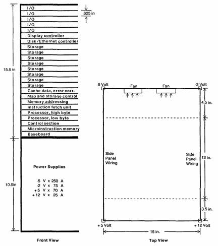
Figure 1a: Dorado chassis
Rather than putting processing capability in each I/O controller and using a shared bus or a switch to access the memory, the Dorado shares the processor among all the I/O devices and the emulator. This fundamental concept of the architecture, which motivates much of the processor design, was first tried in the Alto. It works for two main reasons.
* First, unless a system has both multiple memory busses (i.e., multi-ported memories) and multiple memory modules which can cycle independently, the main factor governing processor throughput is memory contention. Put simply, when I/O interfaces make memory references, the emulator ends up waiting for the memory. In this situation the processor might as well be working for the I/O device.
* Second, when the processor is available to each device, complex device interfaces can be implemented with relatively little dedicated hardware, since most of the control does not have to be duplicated in each interface. For low bandwidth devices, the force of this argument is reduced by the availability of LSI controller chips, but for data rates above one megabit/ second no such chips exist as yet.
Of course, to make this sharing feasible, switching the processor must be nearly free of overhead, and devices must be able to make quick use of the processor resources available to them.
Many design decisions are based on the need for speed. Raw circuit speed is a beginning. Thus, the Dorado is implemented using the fastest commercially available technology which has a reasonable level of integration and is not too hard to package. In 1976, the obvious choice was the ECL 10K family of circuits; probably it still is. Secondly, the processor is organized around two pipelines. One allows a microinstruction to be started in each cycle, though it takes three cycles to complete execution. Another allows a processor context switch in each cycle, though it takes two cycles to occur. Thirdly, independent busses communicate with the memory, IFU, and I/O systems, so that the processor can both control and service them with minimal overhead.
Finally, the design makes the processor both accessible and flexible for users at the microcode level, so that when new needs arise for fast primitives, they can easily be met by new microcode. In particular, the hardware eliminates constraints on microcode operations and sequencing often found in less powerful designs, e.g., delay in the delivery of intermediate results to registers or in calculating and using branch conditions, or pipeline delays that require padding of microinstruction sequences without useful work. We also included an ample supply of resources: 256 general registers, four hardware stacks, a fast barrel shifter, and fully writeable microstore, to make the Dorado reasonably easy to microcode.
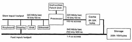
Figure 1b: Dorado block diagram
5. Low level architecture
This section describes in some detail the key ideas of the architecture. Implementation techniques and details are for the most part deferred to the next section; readers may want to jump ahead to see the application of these ideas in the processor. Along with each key idea is a reference to the places in the processor where it is used.
5.1 Tasks
There are 16 priority levels associated with microcode execution. These levels are called microtasks, or simply tasks. Each task is normally associated with some hardware and microcode which together implement a device controller. The tasks have a fixed priority, from task 0 (lowest) to task 15 (highest). Device hardware can request that the processor be switched to the associated task; such a wakeup request will be honored when no requests of higher priority are outstanding. The set of wakeup requests is arbitrated within the processor, and a task switch from one task to another occurs on demand.
When a device acquires the processor (that is, the processor is running at the requested priority level and executing the microcode for that task), the device will presumably receive service from its microcode. Eventually the microcode will block, thus relinquishing the processor to lower priority tasks until it next requires service. While a given task is running, it has the exclusive attention of the processor. This arrangment is similar in many ways to a conventional priority interrupt system. An important difference is that the tasks are like coroutines or processes, rather than subroutines: when a task is awakened, it continues execution at the point where it blocked, rather than restarting at a fixed point. This ability to capture part of the state in the program counter is very powerful.
Task 0 is not associated with a device controller; its microcode implements the emulators currently resident in the Dorado. Task 0 requests service from the processor at all times, but with the lowest priority.
5.2 Task scheduling
Whenever resources (in this case, the processor) are multiplexed, context switching must only happen when the state being temporarily abandoned can be restored. In most multiplexed microcoded systems, this requires the microcode itself to explicitly poll for requests, save and restore state, and initiate context switches. A certain amount of overhead results. Furthermore, the presence of a cache introduces large and unpredictable delays in the execution of microcode (because of misses). A polling system would leave the processor idle during these delays, even though the work of another task can usually proceed in parallel. To avoid these costs, the Dorado does task switching on demand of a higher priority device, much like a conventional interrupt system. That is, if a lower priority task is executing and a higher priority device requests a wakeup, the lower priority task will be preempted; the higher priority device will be serviced without the knowledge or consent of the currently active task. The polling overhead is absorbed by the hardware, which also becomes responsible for resuming a preempted task once the processor is relinquished by the higher priority device. A controller will continue to request a wakeup until notified by the processor that it is about to receive service; it then removes the request, unless it needs more than one unit of service. When the microcode is done, it executes an operation called BLOCK which releases the processor. The effect is that requesting service is done explicitly by device controllers, but scheduling of a given task is invisible to the microcode (and nearly invisible to the device hardware).
5.3 Task specific state
In order to allow the immediate task switching described above, the processor must be able to save and restore state within one microcycle. This is accomplished by keeping the vital state information throughout the processor not in a single rank of registers but in task specific registers.. These are actually implemented with high speed memory that is addressed by a task number. Examples of task specific registers are the microcode program counter, the branch condition register, the microcode subroutine link register, the memory data register, and a temporary storage register for each task. The number of the task which will execute in the next microcycle is broadcast throughout the processor and used to address the task specific registers. Thus, data can be fetched from the high speed task specific memories and be available for use in the next cycle.
Not all registers are task specific. For example, COUNT and Q (described later) are normally used only by task 0. However, they can be used by other tasks if their contents are explicitly saved and restored after use.
5.4 Pipelining
There are two distinct pipelines in the Dorado processor. The main one fetches and executes microinstructions. The other handles task switching, arbitrates wakeup requests, and broadcasts the next task number to the rest of the Dorado. Each structure is synchronous, and there is no waiting between stages.
The instruction pipeline, illustrated in figure 2, requires three cycles (divided into six half cycles) to completely execute a microinstruction. The first cycle is used to fetch it from microstore (time t-2 to t0). The result of the fetch is loaded into the microinstruction register MIR at t0. The second cycle is split; in the first half, operand fetches (as dictated by the contents of MIR) are performednd the results latched at tt in two registers (a and B) which form inputs to the next stage. In the second half cycle, the alu operation is begun. It is completed in the first half cycle of cycle three, and the result is latched in register RESULT (at t3). The second half of cycle three (t3 to t4) is used to load results from RESULT into operand registers.
The figure also shows how the pipeline overlapping is achieved. A new microinstruction begins at every cycle time. The operand registers are used in the first half cycle of every cycle to fetch operands for the current instruction (during t0-t1). The second half of every cycle is used to store results for the previous instruction (during t3-t4).
Figure 3 shows the task arbitration pipeline. This pipeline is two stages long, and also requires one cycle per stage. At the beginning of the pipeline (t0), wakeup requests from device controllers are latched into the WAKEUP register. During the first half cycle (t0-t1), arbitration is performed and the highest priority task determined. During the second half cycle (t1-t2). the microprogram address for the highest priority task is fetched from the task specific program counter TPC. The task number, its TPC, and the command to switch tasks (if the highest priority task is higher than the currently executing task) are loaded into registers at t2. In the second pipe cycle, the TPC is used to fetch the next microinstruction from the microstore, the entire processor uses the selected task number to fetch the appropriate task specific information, and device controllers are told which task will have the processor next. Finally, at t4 the task switch is complete, and the new task is in control of the processor; this time corresponds to t0 of the first microinstruction executed by the new task.
151
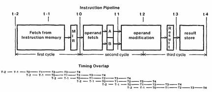
Figure 2: Instruction pipeline and timing overlap
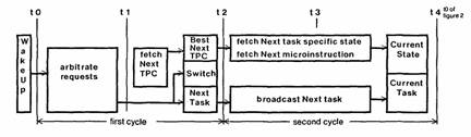
Figure 3: Task arbitration pipeline
5.5 Microinstruction format
One of the key decisions made in the design of any microprogrammed processor is the format and semantics of the microinstruction. The Dorado’s demand for compactness and power are at odds in this case. Compactness dictates that an essentially vertical structure be used, with encoded fields specifying many functions in a few bits. The details of the microinstruction format appear in § 6. The major features of interest here are the choice of successor instruction encoding, and the specification of a large number of functions which may be executed by the processor.
In a classical microprogrammed processor, each instruction carries with it the address of its successor, NextPC; this address is latched with the rest of the instruction, and then used directly to address the microstore for fetching the next instruction. NextPC may be modified by state within the processor during execution, but the basic idea is that enough bits must be present in each microword to address the whole microstore. This results in a uniform structure for addressing, and allows the next instruction fetch to proceed without any delay for decoding; it has the disadvantages of increasing the size and cost (and reducing the speed) of the microstore. The lack of any decoding time also makes it impossible to specify a subroutine return or other major change in sequencing, and have it take effect immediately (branches can still use the scheme described below).
The alternative, which we make use of in the Dorado, is to divide the microstore into pages, use a few bits to specify a next address within the current page, and have a type field which can specify branches, calls, returns, transfers to another page, or whatever. At the start of a micro-cycle, the processor decodes the type field and accesses other information (such as the current page number or the return link) to compute NextPC. In addition, some types cause side effects such as loading the return link. The net result is substantially fewer bits to control microsequencing than a horizontal scheme would require (in the Dorado, 8 bits instead of about 16). The disadvantages are, of course, the cost and time for decoding this field, and the additional complexity of an assembler that can fit instructions onto pages appropriately.
Conditional branching is always a problem with pipelined instruction execution. Many designs incorporate one of the following two schemes; both have drawbacks that we have avoided. The first requires that a branch be specified one (or more) instructions before it is taken. Although this simplifies and speeds up the hardware, it imposes severe constraints on the microcode organization, and often forces extra instructions to be executed. The second scheme detects the branch and inserts asynchronous delay or an extra cycle to allow time for the new instruction to be fetched. This obviously slows down the machine.
Conditional branching in the Dorado is handled by allowing one of eight branch conditions to modify the low order bit of NextPC. This modification (Boolean or into the low order bit) takes place about halfway into the instruction fetch cycle. The microstore is organized so that this bit does not change the chip address, but instead selects a different chip from a set of chips whose outputs are tied directly together. Since access time via the “chip select” is considerably faster than from the address, the late arriving branch condition does not increase the total cycle time. For this to work, the assembler must place each false branch target at an even address, and the corresponding true branch target at the next higher odd address. An annoying consequence is that several conditional branches cannot have the same target; when this case arises the target must be duplicated. Everything has its price.
Another tradeoff occurs in the mechanism for controlling the functions of the processor at each microcycle. The Dorado encodes most of its operations (other than register selection, ALU operations, storing results, and memory references) in an eight bit function field called FF. This is quickly decoded at the beginning of every microinstruction execution cycle (during t0-t1), and is used to invoke all of the less frequently used operations that the processor can do: controlling the I/O busses, reading and setting state in the memory and IFU, extracting an arbitrary field from a word, reading and loading most registers, non-standard carry and shift operations, and loading values into small registers. FF can also serve as an eight bit constant or as part of a full microstore address. This encoding saves many bits in the microinstruction, at the expense of allowing only one FF-specified operation to be done in each cycle, even though the data paths exist for doing many such operations in parallel.
5.6 Data bypassing
Recall that a microinstruction is initiated at the beginning of every cycle, but takes one cycle for instruction fetch, and two cycles for execution. If an instruction uses a result generated by its immediate predecessor, it needs to get that result from an operand register before the predecessor has actually delivered the result to that register. Rather than forbidding such use of results, or delaying execution until the register has been loaded, we solved this problem with a technique called bypassing. The hardware detects that an operand specified in the current instruction is actually the result of the previous instruction. Rather than obtaining the operand from the usual source in a RAM, the processor takes it directly from the input to the RAM, which is the result of the previous instruction. Figure 4 illustrates the scheme. This costs extra hardware for multiplexors and bypass detection logic, but the result is much smaller and faster microcode in many common cases. In the Model 0 Dorado, we omitted bypassing logic in a few places, and required the microcoder to avoid these cases. The result was a number of subtle bugs and a significant loss of performance.
5.7 Memory delays
Pipelining and bypassing are effective ways to reduce delay and increase throughput within the processor. Interactions with the memory, however, pose different problems. Once a memory reference has been made, there must be some way to tell when the memory system has delivered the requested data. Two simple techniques are to wait a fixed (unfortunately, maximum) amount of time before using the data, or to explicitly poll the memory system. Neither is satisfactory for a high performance machine. First, the difference between the best case (cache hit) and the worst (cache miss plus memory system resource contention) is more than an order of magnitude. Second, useful work can often be performed by a given task before it uses the requested memory data. Third, even if a given task must wait for memory data before it can proceed, higher priority tasks may very well be able to do useful work in the meantime.
The Dorado manages this problem by making the memory keep track of when data is ready, and allowing the processor to continue executing instructions [1]. Only instructions which use memory data or start memory references can be affected by the state of the memory. When such an instruction is executed, the memory checks to see whether it can be allowed to proceed. If so, no action is taken. But if the memory is busy, or the data being used is not ready, the memory responds by activating the signal HOLD. The effect of HOLD is to stop any state changes specified by the current instruction. However, all the clocks in the system keep running. This is important, because task switching must not be inhibited during memory delays. In effect, HOLD converts the currently executing instruction into a “no operation, jump to self instruction. If no task switch occurs, the instruction is executed again, and a new calculation is made to see whether it can proceed. Meanwhile, the memory pipeline is running, and sooner or later, the need for HOLD will be gone as the pipeline progresses.
Note that if a task switch occurs while an instruction is held, the state is such that the held instruction may simply be restarted when the lower priority task is resumed by the processor. Cycles which would otherwise be dead time are consumed instead by higher priority tasks doing useful work.
5.8 Separate external interfaces
If most macroinstructions (byte codes) are to execute in a small number of cycles, hardware must be provided to make communication among processor, IFU, and memory very quick in the common cases. The Dorado provides a number of data paths and control structures for this purpose, detailed in the block diagrams, figures 5 and 6. All the busses are a full word wide and can be accessed in one cycle or less. The B input to the ALU is extended to the remainder of the Dorado (except the I/O devices, which have their own busses) for the transfer of status and control between the processor and the other subsystems. The memory address bus is a copy of the A side ALU input. Memory data comes directly into the processor and is routed to a variety of destinations simultaneously, to make such operations as field manipulations and indirect addressing fast. The IFU can directly supply operand data to the processor, and any microinstruction can specify that it is the last of a macroinstruction, in which case the successor address is supplied by the IFU. This requires a microstore address bus and operand data bus directly from the IFU to the processor.
It is also desirable to make I/O transfers through the processor. To this end there is an I/O address and a data bus for direct access to I/O controllers. The data bus can transfer one word per cycle, or 320 Mbits/second, and both the memory reference and the I/O transfer can be specified in a single instruction, so that it is possible to move a sequence of words between the cache and a device at this rate. However, this subsystem is called the slow I/O system. There is also a more direct memory access I/O subsystem, the fast I/O system; it allows data to move directly between memory and I/O devices, in blocks of 16 words, without polluting the cache memory. Figure 1b shows a display controller that uses both slow and fast I/O systems.
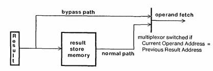
Figure 4: Bypassing example
5.9 Constants
Notice that there is no source for 16 bit constants within the processor. Such constants are necessary, particularly in device controller microcode where they often are used as commands, addresses, or literal data. It would be possible to include a constant box, addressed perhaps with an FF function, as a source for constants. However, such a box would have a limited size and, experience tells us, would not hold enough constants to satisfy a growing world.
Fortunately, a large fraction of the constants used in microcoding are either small positive or small negative (2’s complement) integers, or sparsely populated bit vectors, with the property that one of the two eight bit fields in the constant is all zeroes or all ones. Thus a useful subset of constants can be specified using the eight bits of FF for one byte of the constant and two other bits to specify the other byte value and position. Using this technique, most 16 bit constants can be specified in one microinstruction, and any constant can be assembled in two microinstructions. (The “other” two bits come from the BSelect field in the microword.)
6. Implementation
In this section we describe, at the block diagram level, the actual implementation of the Dorado processor. There is only space to cover the most interesting points and to illustrate the key ideas from § 5.
6.1 Clocks
The Dorado has a fully synchronous clock system, with a clock tick every 25 nanoseconds (nominal). A cycle consists of two successive clock ticks; it begins on an even tick, which is followed by an odd tick, and completes coincident with the beginning of a new cycle on the next even tick. Even ticks may be labeled with names like t-2, t0, t2, t4 to denote events within a microinstruction execution or a pipeline, relative to some convenient origin. Odd ticks are similarly labeled t-1; t1, t3.
6.2 The control section
The processor can be divided into two distinct sections, called control and data. The control section fetches and broadcasts the microinstructions to the data section (and the remainder of the Dorado), handles task switching, maintains a subroutine link, and regulates the clock system. It also has an interface to a console and monitoring microcomputer which is used for initialization and debugging of the Dorado. Figure 5 is a block diagram of the control section.
6.2.1 Task pipeline
The task pipeline consists of an assortment of registers and a priority encoder. All the registers are loaded on even clocks. Wakeup requests are latched at t0 in WAKEUP, one bit per task. READY has corresponding bits for preempted and explicitly readied tasks; a task can be explicitly made ready by a microcode function.. The requests in wakeup and READY compete. The priority encoder produces the number of the highest priority task, which is loaded into BestNextTask and also used to read the TPC of this task into BestNextPC; these registers are the interface between the two stages in this pipeline. The NEXT bus normally gets the larger of BestNextTask and CurrentTask. CurrentTask is loaded from NEXT, and Previous-Task is loaded from CurrentTask, as the pipeline progresses.
This method of priority scheduling means that once a task is initiated, it must explicitly relinquish the processor before a lower priority task can run. A bit in the micro-word, BLOCK, is used to indicate that NEXT should get BestNextTask unconditionally (unless the instruction is held).
Note that it takes a minimum of two cycles from the time a wakeup changes to the time this change can affect the running task (one for the priority encoding, one to fetch the microinstruction). This implies that a task must execute at least two microinstructions after its wakeup is removed before it blocks; otherwise it will continue to run, since the effects of its wakeup will not have been cleared from the pipe. The device cannot remove the wakeup until it knows that the task will run (by seeing its number on NEXT). Hence the earliest the wakeup can be removed is t0 of the first instruction (NEXT has the task number in the previous cycle, and the wakeup is latched at t0); thus the grain of processor allocation is two cycles for a task waking up after a BLOCK.
Some trouble was taken to keep the grain small, for the following reason. Since the memory is heavily pipelined and contains a cache which does not interact with high bandwidth I/O, the I/O microcode often needs to execute only two instructions, in which a memory reference is started and a count is decremented. The processor can then be returned to another task. The maximum rate at which storage references can be made is one every eight cycles (this is the cycle time of the main storage RAMs). A two cycle grain thus allows the full memory bandwidth of 640 Mbits/second to be delivered to I/O devices using only 25% of the processor.
A simpler design would require the microcode to explicitly notify its device when the wakeup should be removed; it would then be unnecessary to broadcast NEXT to the devices. Since this notification could not be done earlier than the first instruction, however, the grain would be three cycles rather than two, and 37.5% of the processor would be needed to provide the full memory bandwidth. Other simplifications in the implementation would result from making the pipeline longer; in particular, since squeezing the priority encoding and reading of TPC into one cycle is quite difficult, these two operations could be more easily done in separate pipe stages. Again, however, this would increase the grain.
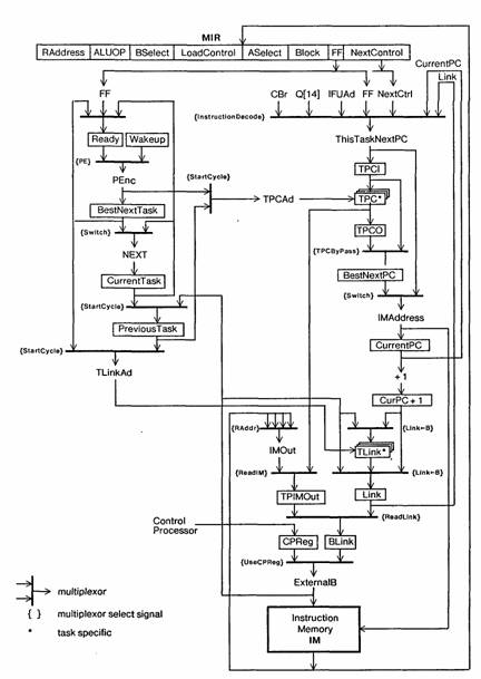
Figure 5: Control section
6.2.2 Fetching microinstructions
Refer to the right hand side of figure 5. At t0 of every instruction, the microinstruction register MIR is loaded from the outputs of IM, the microinstruction memory, and the CurrentPC register is loaded with IMAddress. The NextPC is quickly calculated based on the NextControl field in MIR, which encodes both the instruction type and some bits of NextPC; see figure 7 for details. This calculation produces ThisTaskNcxtPC, so called because if a task switch occurs it is not used as the next IMAddress. Instead, the BestNextPC computed in the task pipeline is used as IMAddress.
tpc is written with the previous value of ThisTaskNextPC every cycle (at t3), and read for the task in BestNextTask every cycle as well. Thus, TPC is constantly recording the program counter value for the current task, and also constantly preparing the value for the next task in case there is a task switch.
6.2.3 Miscellaneous features
There is a task specific subroutine linkage register, LINK, shown in figure 5, which is loaded with CurrentPC + 1 on every microcode call or return. Thus each task can have its own microcoded coroutines. LINK can also be loaded from a data bus, so that control can be sent to an arbitrary computed address; this allows a microprogram to implement a stack of subroutines, for example. In addition to conditional branches, which select one of two NextPC values, there are also eight-way and 256-way dispatches, which use a value on the B bus to select one of eight, or one of 256 NextPC values.
There are data paths for reading and writing microstore. Related paths allow reading and writing TPC. These paths (through the register TPIMOut) are folded into already existing data paths in the control section and are somewhat tortuous, but they are used infrequently and hence have been optimized for space. In addition, another computer (either a separate microcomputer or an Alto) serves as the console processor for the Dorado; it is interfaced via the CPREG and a very small number of control signals.
6.3 The data section
Figure 6 is a block
diagram of the data section, which is organized around an arithmetic/logic unit
(ALU) in the usual way. It implements most of the registers accessible to the
programmer and the microcode functions for selecting operands, doing operations
in the ALU and shifter, and storing results. It also calculates branch
conditions, de— codes MIR fields and broadcasts decoded signals to the rest of
the Dorado, supplies and accepts memory addresses and data, and supplies I/O
data and addresses.
6.3.1 The microinstruction register
MIR (which actually belongs to the control section) is 34 bits wide and is partitioned into the following fields:
RAddress 4 Addresses the register bank RM.
ALUOP 4 Selects the ALU operation or controls the shifter.
BSelect 3 Selects the source for the B bus, including constants.
LoadControl 3 Controls loading of RM and T.
ASelect 3 Selects the source for the A bus, and starts memory references.
BLOCK 1 Blocks an I/O task, selects a stack operation for task 0.
FF 8 Catchall for specifying functions.
NextControl 8 Specifies how to compute NextPC.
6.3.2 Busses
The major busses are A, B (alu sources), RESULT, External, MemAddress, IOAddrcss, lOData, IFUData, and MemData.
The ALU accepts two inputs (A and B) and produces one output (RESULT). The input busses have a variety of sources, as shown in the block diagram. RESULT usually gets the alu output, but it is also sourced from seven other places, including a one bit shift in either direction of the ALU output. A copy of A is used for MemAddress; two copies of B are used for ExternalB and IOData. MemAddress provides a 16 bit displacement, whic’h is added to a 28 bit base register in the memory system to form a virtual addresses. Externals is a copy of B which goes to the control, memory, and IFU sections, and IOData is another copy which goes to the I/O system; the sources of B can thus be sent to the entire processor. Both are bidirectional and can serve as a source for data as well. IOAddress is driven from a task specific register; it specifies the particular device and register which should source or receive lOData.
IFUData and MemData allow the processor to receive data from the IFU and memory in parallel with other data transfers. MemData has the value of the memory word most recently fetched by the current task; if the fetch is not complete, the current task is held when it tries to use MemData. IFUData has an operand of the current macro-instruction; as each operand is used, the IFU presents the next one on IFUData.
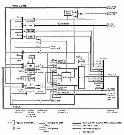
Figure 6: Data section
6.3.3 Registers
Here is a list and brief description of registers seen by the microprogrammer. All are one word (16 bits) wide.
RM: a bank of 256 general purpose registers; a register can be read onto A, B, or the shifter, and loaded from RESULT under the control of LoadControl. Normally, the same register is both read and loaded in a given microinstruction, but loading of a different register can be specified by FF.
STACK: a memory addressed by the StackPtr register. A word can be read or written, and StackPtr adjusted up or down, in one microinstruction. If STACK is used in a microinstruction, it replaces any use of RM, and the RAddress field in the microword tells how much to increment or decrement StackPtr. The 256 word memory is divided into four 64 word stacks, with independent underflow and overflow checking.
T: a task specific register used for working storage; like RM, it can be read onto A, B, or the shifter, and loaded from RESULT under the control of LoadControl.
COUNT: a counter; it can be decremented and tested for zero in one microinstruction, using only the Next-Control or FF field. It is loaded from B or with small constants from FF.
Q: a hardware aid for multiply and divide instructions; it can be read onto A or B, and loaded from B, and is automatically shifted in useful ways during multiply and divide step microinstructions.
The registers in the next group vary in width. They are used as control or address registers, changed dynamically but infrequently by microcode.
RBase: a task specific base register for RM. RM addressing requires eight bits. Four come from the RAddress field in the microword, and the other four are supplied from RBase. It is loaded from B or FF, and can be read onto RESULT.
StackPtr: an eight-bit register used as a stack pointer. Two bits of StackPtr select a stack, and the least significant six bits a word in the stack. The latter bits are incremented or decremented under control of the RAddress field whenever a stack operation is specified.
MemBase: a task specific five-bit register which selects one of 32 base registers in the memory to be used for virtual address calculation. It is loaded from FF or from B, and can be loaded from the IFU at the start of a macroinstruction.
ALUFM: a 16 word memory which maps the four-bit ALUOP field into the six bits required to control the ALU.
IOAddress: a task specific register which drives the IOAddress bus, and is loaded by I/O microcode to specify a device address for subsequent INPUT and OUTPUT operations. It may be loaded from B or FF.
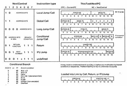
Figure 7: Next address formation
6.3.4 The shifter
The Dorado has a 32 bit barrel shifter for handling bit-aligned data. It takes 32 bits of input from RM and T, performs a left cycle of any number of bit positions, and places the result on A. The ALU output may be masked during a shift instruction, either with zeroes or with data from MemData.
The shifter is controlled by a register called ShiftControl. To perform a shift operation, ShiftControl is loaded (in one of a variety of ways) with control information, and then one of a group of “shift and mask” micro-operations is executed.
6.4 Physical organization
Once the goal of a physically small but powerful machine was established, engineering design and material lead times forced us to develop the Dorado package before the logic design was completed, and the implementation then had to fit the package. The data section is partitioned onto two boards, eight bits on each; the boards are about 70% identical. The control section divides naturally into one board consisting of all the IM chips (high speed 1K x 1 bit ECL RAMs) and their associated address drivers, and a second board with the task switch pipeline, NextPC logic, and LINK register.
The sidepanel pins are distributed in clusters around the board edges to form the major busses. The remaining edge pins are used for point to point connections between two specific boards. The I/O busses go uniformly to all the I/O slots, but all the other boards occupy fixed slots specifically wired for their needs. Half the pins available on the sideplanes are grounded, but wire lengths are not controlled except in the clock distribution system, and no twisted pair is used in the machine except for distribution of one copy of the master clock to each board.
We were very concerned throughout the design of Dorado to balance the pipelines so that no one pipe stage is significantly longer than the others. Furthermore, we worked hard to make the longest stage (which limits the speed of this fully synchronous machine) as short as possible. The longest stage in the processor, as one might have predicted, is the IMAddress calculation and microinstruction fetch in the control section. There is about a 50 nanosecond limit. There are pipe stages of about the same length in the memory and IFU.
We also worked hard to get the most out of the available real estate, by hand tailoring the integrated circuit layout and component usage, and by incrementally adding function until nearly the entire board was in use. We also found that performance could be significantly improved by careful layout of critical paths for minimum loading and wiring delay. Although this was a very labor intensive operation, we believe it has paid off.
7. Performance
Four emulators have been implemented for the Dorado, interpreting the Bcpl, Lisp, Mesa, and Smalltalk instruction sets. A typical microinstruction sequence for a load or store instruction takes only one or two microinstructions in Mesa (or Bcpl), and five in Lisp. The Mesa opcode can send a 16 bit word to or from memory in one microinstruction; Lisp deals with 32 bit items and keeps its stack in memory, so two loads and two stores are done in a basic data transfer operation. More complex operations (such as read/write field or array element) take five to ten microinstructions in Mesa and ten to twenty in Lisp. Note that Lisp does runtime checking of parameters, while in Mesa most checking is done at compile time. Function calls take about 50 microinstructions for Mesa and 200 for Lisp.
The Dorado supports raster scan displays which are refreshed from a full bitmap in main memory; this bitmap has one bit for each picture element (dot) on the screen, for a total of .5-1 Mbits. A special operation called BitBlt (bit boundary block transfer) makes it easier to create and update bitmaps; for more information about BitBlt consult [9], where it is called RasierOp. BitBlt makes extensive use of the shifting/masking capabilities of the processor, and attempts to prefetch data so that it will always be in the cache when needed. The Dorado’s BitBlt can move display objects around in memory at 34 Mbits/sec for simple cases like erasing or scrolling a screen. More complex operations, where the result is a function of the source object, the destination object, and a filter, run at 24 Mbits/ sec.
I/O devices with transfer rates up to 10 Mwords/sec are handled by the processor via the IOData and IOAddress blisses. The microcode for the disk takes three microinstructions to transfer two words in this way; thus the 10 Mbit/sec disk consumes 5% of the processor. Higher bandwidth devices use the fast I/O system, which does not interact with the cache. The fast I/O microcode for the display takes only two instructions to transfer a 16 word block of data from memory to the device. This can consume the available memory bandwidth for I/O (640 Mbits/sec) using only one quarter of the available microcycles (that is, two I/O instructions every eight cycles).
Recall that the NextPC scheme (§ 5.5 and § 6.2.2) imposes a rather complicated structure on the microstore, because of the pages, the odd/even branch addresses, and the special subroutine call locations. We were concerned about the amount of microstore which might be wasted by automatic placement of instructions under all these constraints. In fact, however, the automatic placer can use 99.9% of the available memory when called upon to place an essentially full microstore.
8. Current status
The processor for the Model 1 Dorado has been in operation since winter of 1978-79. Several copies of the completed machine were delivered to users in CSL during the summer and fall of 1979. We are converting the manufacturing technology for Dorado from the stitchweld boards used for the prototypes to MultiWire boards. Stitch welding worked very well for prototypes, but is too expensive for even modest quantities. Its major advantages are packaging density and signal propagation characteristics very similar to those of the production technology, very rapid turnaround during development (three days for a complete 300-chip board, a few hours for a modest change), and complete compatibility with our design automation system.
Acknowledgements
The early design of the Dorado processor was done by Chuck Thacker and Don Charnley. The data section was redesigned and debugged by Roger Bates and Ed Fiala. Willie-Sue Haugeland, Nori Suzuki, Bruce Horn and Gene McDaniel are responsible for production and diagnostic microcode.
References
1. Lampson, B.W., Clark, D.W. and Pier, K.A. The memory system of a high-performance personal computer. Xerox parc, in preparation.
2. Deutsch, L.P. Experience with a microprogrammed Interlisp system. IEEE. Trans. Computers C-28, 10 (Oct 1979).
3. Geschke, C.M., Morris Jr., J.H., and Satterthwaite, E.H. Early experience with Mesa. Comm ACM 20, 8 (Aug 1977), 540-552.
4. Ingalls, D. The Smalltalk-76 programming system: Design and implementation. Proc 5th ACM Symp. Principles of Prog. Lang., Tucson, Arizona. Jan 1978, 9-16.
5. Iampson, B.W., McDaniel, G. and Ornstein, S. An instruction fetch unit for a high-performance personal computer. Xerox PARC, in preparation.
6. Mitchell, J.G., Maybury, W. and Sweet, R. Mesa Language Manual, Technical Report CSL-79-3, Xerox PARC, 1979.
7. Teitelman, W. Interlisp Reference Manual, Xerox parc, 1979.
8. Thackcr, C.P. et al. Alto: A personal computer. Computer Structures: Readings and Examples, Sieworek, Bell and Newell, eds., McGraw-Hill, 1980.
9. Newman, W.M. and Sproull, R.F. Principles of Interactive Computer Graphics, 2nd Ed. McGraw-Hill, 1979.